Semiconductor device

a semiconductor and device technology, applied in the field of semiconductor devices, can solve the problems of high parasitic capacitance, large harmonic distortion, and high cost of compound semiconductor substrates with excellent rf characteristics, and achieve the effect of reducing the cost of antenna switches and minimizing the harmonic distortion generated in antenna switches

Active Publication Date: 2011-12-29
RENESAS ELECTRONICS CORP
View PDF9 Cites 64 Cited by
  • Summary
  • Abstract
  • Description
  • Claims
  • Application Information

AI Technical Summary

Benefits of technology

[0014]In terms of achieving a reduction in the cost of an antenna switch, even when the antenna switch is particularly formed of

Problems solved by technology

However, a compound semiconductor substrate having an excellent RF characteristic is costly, and is not desirable in terms of a reduction in the cost of the antenna switch.
However, the low-cost silicon substrate has the pro

Method used


Image

  • Semiconductor device
  • Semiconductor device
  • Semiconductor device

Examples


first embodiment

Structure and Operation of Mobile Phone

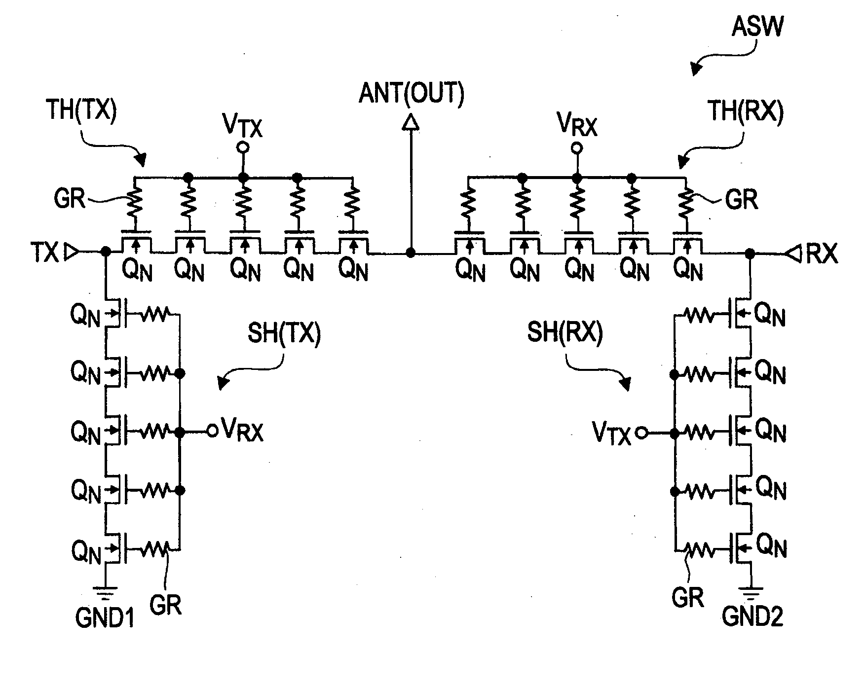
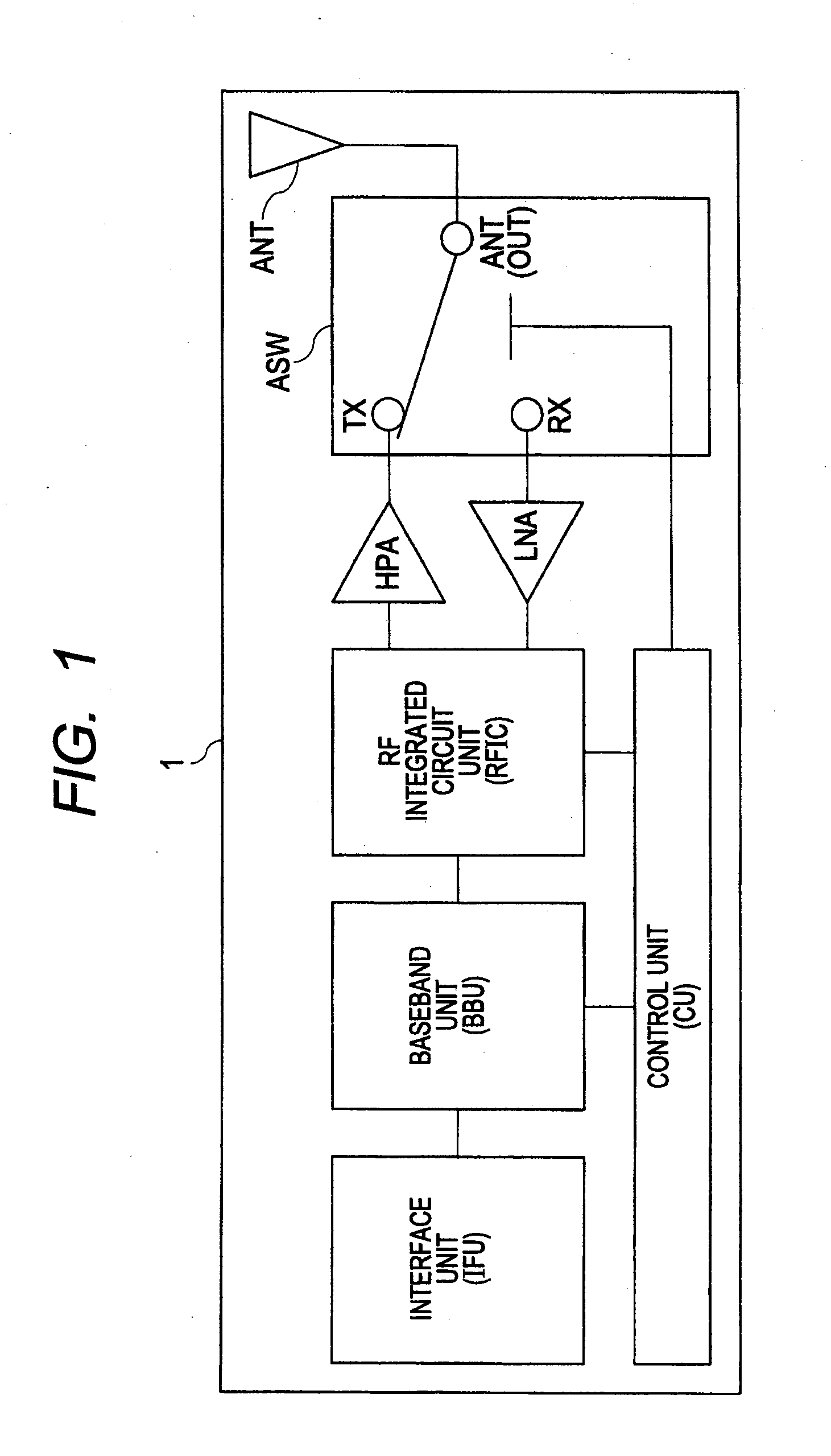
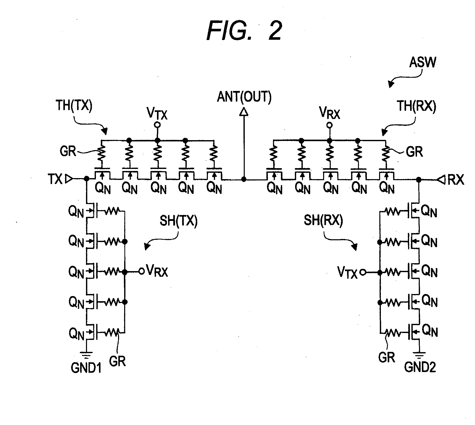
[0057]FIG. 1 is a block diagram showing a structure of the transmission / reception unit of a mobile phone. As shown in FIG. 1, a mobile phone 1 has a control unit CU, an interface unit IFU, a baseband unit BBU, an RF integrated circuit unit RFIC, a power amplifier HPA, a low noise amplifier LNA, an antenna switch ASW, and an antenna ANT.

[0058]The interface unit IFU has the function of processing an audio signal from a user (caller). That is, the interface unit IFU has the function of providing an interface between the user and the mobile phone. The baseband unit BBU has a CPU as a central control unit embedded therein, and is configured to be capable of, during transmission, digital processing of the audio signal (analog signal) from the user (caller) via an operation unit to generate a baseband signal. The baseband unit BBU is also configured to be capable of, during reception, generation of the audio signal from the baseband signal which is a ...

second embodiment

Application of Distortion Compensating Capacitance Circuit in Second Embodiment to Antenna Switch

[0224]In the foregoing first embodiment, the description has been given to the example in which, between the respective source regions and the respective drain regions of the plurality of MISFETs QN1 to QN5 included in the RX through transistor TH(RX), the distortion compensating capacitance circuits CAPC2 are provided. In the present second embodiment, a description will be given to a configuration in which the plurality of distortion compensating capacitance circuit CAPC2 are coupled in series between the antenna terminal ANT(OUT) provided with the RF through transistor TH(RX) and the reception terminal RX.

[0225]FIG. 21 is a circuit diagram showing a circuit configuration of the RX through transistor TH(RX) provided with the distortion compensating capacitance circuits CAPC2 in the present second embodiment. As shown in FIG. 21, between the antenna terminal ANT(OUT) and the reception t...

third embodiment

[0241]In the distortion compensating capacitance circuit CAPC2 in the first embodiment, the MOS diode capacitance elements MDC1 and MDC2 are coupled in anti-series so as to electrically couple the electrode EL1 of the MOS diode capacitance element MDC1 to the electrode EL2 of the MOS diode capacitance element MDC2. By contrast, in the present third embodiment, a description will be given to a distortion compensating capacitance circuit in which the MOS diode capacitance elements MDC1 and MDC2 are coupled in anti-series so as to electrically couple the semiconductor region NR1B of the MOS diode capacitance element MDC1 to the semiconductor region NR2B of the MOS diode capacitance element MDC2.

[0242](Distortion Compensating Capacitance Circuit in Third Embodiment)

[0243]FIG. 23(a) is a view showing a structure of a distortion compensating capacitance circuit CAPC3 in the present third embodiment. As shown in FIG. 23(a), the distortion compensating capacitance circuit CAPC3 in the prese...


PUM


Abstract

In terms of achieving a reduction in the cost of an antenna switch, there is provided a technology capable of minimizing harmonic distortion generated in the antenna switch even when the antenna switch is particularly formed of field effect transistors formed over a silicon substrate. Between the source region and the drain region of each of a plurality of MISFETs coupled in series, a distortion compensating capacitance circuit is coupled which has a voltage dependency such that, in either of the cases where a positive voltage is applied to the drain region based on the potential of the source region and where a negative voltage is applied to the drain region based on the potential of the source region, the capacitance decreases to a value smaller than that in a state where the potential of the source region and the potential of the drain region are at the same level.

Description

CROSS-REFERENCE TO RELATED APPLICATIONS[0001]The disclosure of Japanese Patent Application No. 2010-147714 filed on Jun. 29, 2010 including the specification, drawings and abstract is incorporated herein by reference in its entirety.BACKGROUND[0002]The present invention relates to a semiconductor device, and particularly to a technology which is effective when applied to a semiconductor device including an antenna switch mounted in, e.g., wireless communication equipment.[0003]In Japanese Unexamined Patent Publication No. 2009-194891 (Patent Document 1), it is described that the voltage dependency of a parasitic capacitance, which is the cause of a third harmonic wave generated from an antenna switch, is compensated for by incorporating a capacitance circuit having an opposite voltage dependency in the antenna switch to reduce third harmonic distortion.RELATED ART DOCUMENTPatent DocumentPatent Document 1[0004]Japanese Unexamined Patent Publication No. 2009-194891SUMMARY[0005]To rece...

Claims


Application Information

Patent Timeline
IPC IPC(8): H01L29/94
CPCH04B1/48H01L29/93
Inventor KONDO, MASAOMORIKAWA, MASATOSHIGOTO, SATOSHI
Owner RENESAS ELECTRONICS CORP
Why Eureka
Try Eureka