Annealed wafer, method for producing annealed wafer and method for fabricating device

a technology of annealing wafers and annealing methods, which is applied in the direction of polycrystalline material growth, crystal growth process, after-treatment details, etc., can solve the problems of complex defects of device characteristics, deterioration of oxide dielectric breakdown voltage characteristics, and adverse effects of bmd on device characteristics, etc., to achieve good tddb characteristic, high quality, and the effect of not decreasing strength

Inactive Publication Date: 2012-01-05
SHIN-ETSU HANDOTAI CO LTD
View PDF2 Cites 28 Cited by
  • Summary
  • Abstract
  • Description
  • Claims
  • Application Information

AI Technical Summary

Benefits of technology

[0103]This effect enables the variation in a plane of characteristics of the CCD and CMOS image sensor to be made small.
[0104]As described above, according to the present invention, since the grown-in oxide precipitates and grown-in defects relevant to oxygen, such as COPs and OSFs, do not exist on the surface layer, which is the device operation region, the annealed wafer having a good TDDB characteristic can be provided. In addition, when the anneale

Problems solved by technology

It was proved that defects that are caused by single crystal growth and deteriorate the oxide dielectric breakdown voltage characteristics and device characteristics are complex defects and grown-in defects, such as FPD, ISTD, COP, and OSF nucleus.
This BMD adversely affects device characteristics, such as a junction leakage, when it is generated in the wafer surface, which is a device active region.
As a result, the Va is unevenly distributed in the bulk.
On the other hand, it has been also reported that the grown-in defects, such as COPs and OSF nucleuses, are annihilated by the RTP processing.
This means that, when a very shallow portion of the surface layer is removed by removing the oxide film formed by the oxidization treatment at 1050° C. for 30 minutes, the COPs are not completely annihilated, although the COPs on the surface are annihilated after the RTP processing, and that the COPs of

Method used


Image

  • Annealed wafer, method for producing annealed wafer and method for fabricating device
  • Annealed wafer, method for producing annealed wafer and method for fabricating device
  • Annealed wafer, method for producing annealed wafer and method for fabricating device

Examples


examples 1 to 6

, Comparative Examples 1 to 8

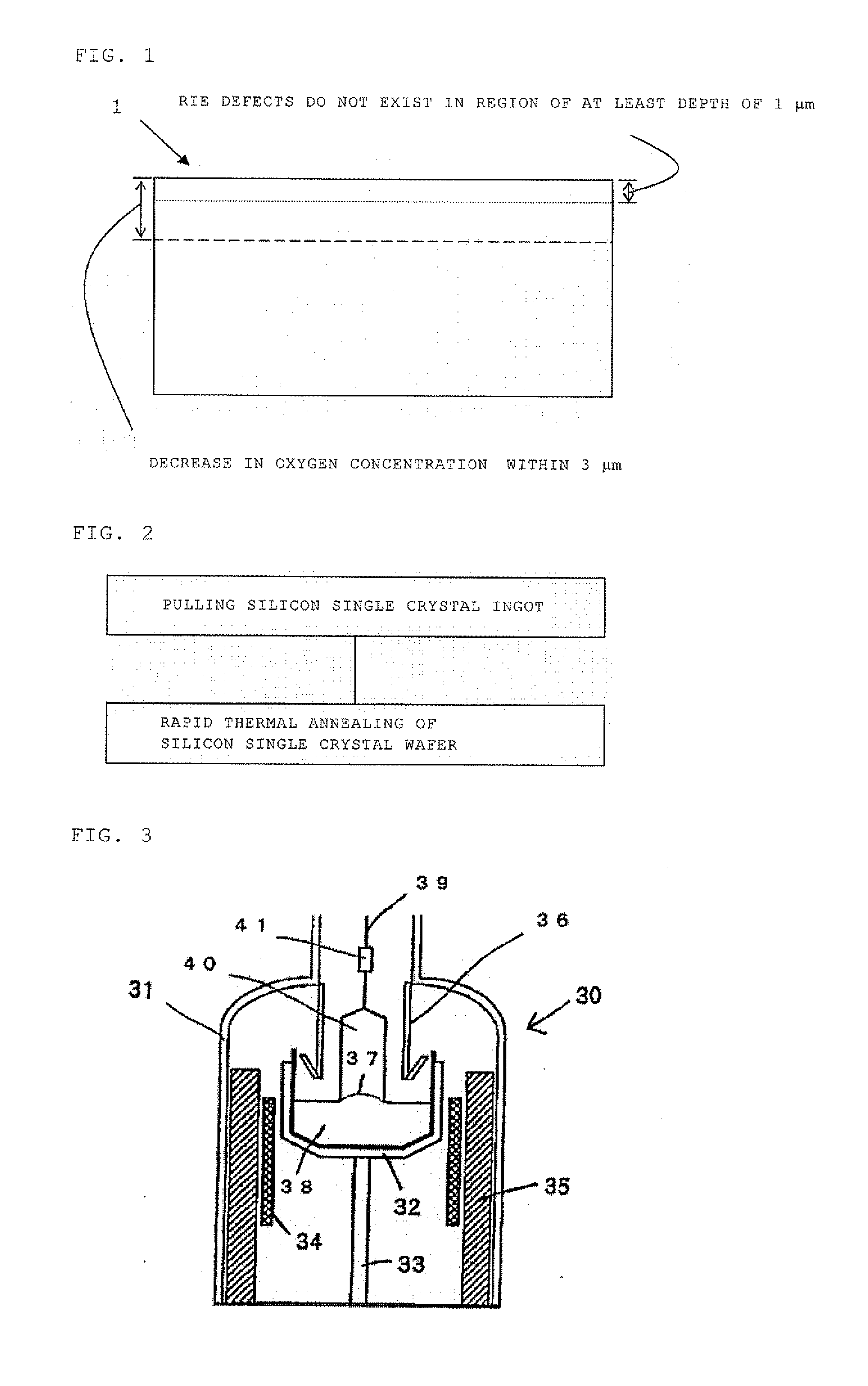
[0203]With the single crystal pulling apparatus shown in FIG. 3, silicon single crystal ingots having various defects regions (a diameter of 12 inches (300 mm), orientation , a conductive type of p-type) were grown while applying a transverse magnetic field by the MCZ method. With the rapidly heating and rapidly cooling apparatus shown in FIG. 5 (here, VANTAGE made by AMAT Inc.), silicon single crystal wafers sliced from the ingots were rapidly heated from a room temperature at a temperature-increasing rate of 50° C. / s under an Ar gas atmosphere, kept at a maximum temperature of 1200 to 1350° C. for 1 to 10 seconds, and thereafter rapidly cooled at a temperature-decreasing rate of 50° C. / s.

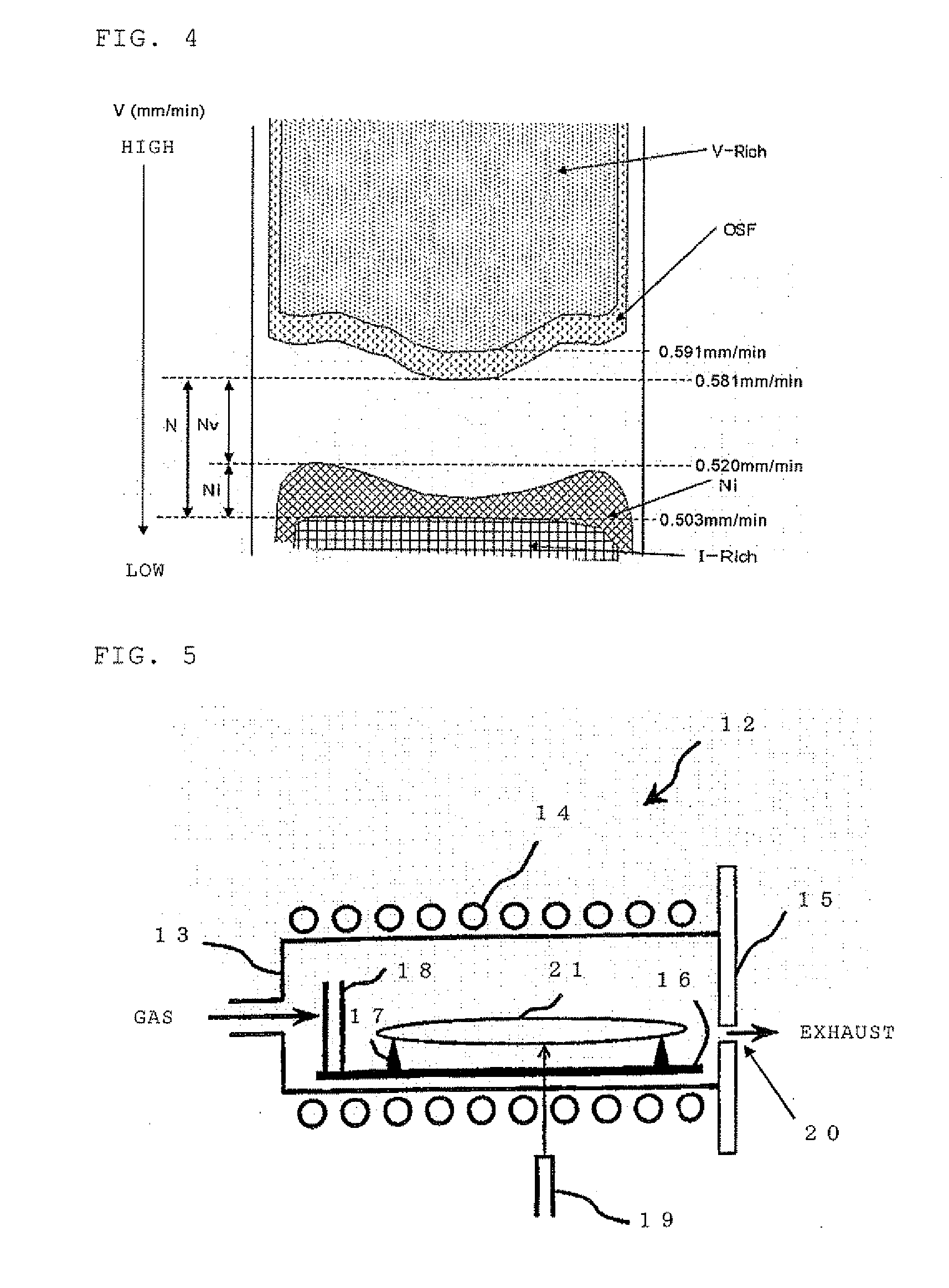
[0204]It is to be noted that the same result as FIG. 4 was obtained in the preliminary examination relevant to the relation between the growth rate and defect region of the silicon single crystal ingot, and the ingots having a desired defect were grown on the basis of ...

example 1

OSF+Nv

[0206]Pulling Rate: 0.585 mm / min, RTP Processing Temperature: 1320° C., RTP Keeping Time: 10 seconds

example 2

OSF+Nv

[0207]Pulling Rate: 0.585 mm / min, RTP Processing Temperature: 1350° C., RTP Keeping Time: 10 seconds


PUM


Abstract

An annealed wafer obtained by performing rapid thermal annealing on a silicon single crystal wafer sliced from a silicon single crystal ingot in which an entire plane is an OSF region, an N region outside an OSF region, or a mixed region thereof, the silicon single crystal ingot being grown by the Czochralski method, in which RIE defects do not exist in a region having at least a depth of 1 μm from a surface, a good chip yield of a TDDB characteristic is 80% or more, and a depth of a region where an oxygen concentration is decreased due to outward diffusion is within 3 μm from the surface, and a method for producing an annealed wafer.

Description

TECHNICAL FIELD[0001]The present invention relates to an annealed wafer having a defect-free region (Denuded zone, hereinafter referred to as a DZ layer) formed thereon, in which grown-in oxide precipitates, grown-in defects, and RIE defects (defects that can be detected by the RIE method) do not exist within a constant depth from a wafer surface, and particularly to an annealed wafer having characteristics that oxide dielectric breakdown voltage is superior, hillocks in a device process can be prevented from being formed, which may be generated in a step of processing a groove with a dry etching apparatus, a decrease in the oxygen concentration due to outward diffusion of the surface is suppressed on the wafer surface, the oxygen concentration distribution is uniform in a depth direction, and a decrease in wafer strength followed by a decrease in the oxygen concentration in the vicinity of a surface layer is suppressed, and to a method for producing the same, and to a method for fa...

Claims


Application Information

Patent Timeline
IPC IPC(8): H01L29/30H01L21/322
CPCH01L21/3225C30B29/06C30B33/02H01L21/02002
Inventor EBARA, KOJIHAYAMIZU, YOSHINORIKIKUCHI, HIROYASU
Owner SHIN-ETSU HANDOTAI CO LTD
Why Eureka
Try Eureka