Miniturization techniques, systems, and apparatus relatng to power supplies, memory, interconnections, and leds

a technology of leds and miniaturization techniques, applied in the direction of generating/distributing signals, coupling device connections, sustainable manufacturing/processing, etc., can solve the problems of power supply design to ensure, improper operation of susceptible components, and several system components to improve performance, and improve functionality. , the effect of miniaturizing the layout of memory and memory controllers

Inactive Publication Date: 2012-01-05
ATD VENTURES
View PDF25 Cites 23 Cited by
  • Summary
  • Abstract
  • Description
  • Claims
  • Application Information

AI Technical Summary

Benefits of technology

[0031]Implementations of the present systems and methods can enable enhanced performance and miniaturized layout of memory and memory controllers. Accordingly, in some aspects, a circuit board is provided having a top and a bottom side. A memory controller is coupled to the circuit board along with a plurality of memory devices. To improve functionality and decrease footprint, the memory devices are soldered (or otherwise electrically connected) directly to the circuit board on both the top and bottom sides of the board. In this manner, each of the memory devices can be located within about 6.4 centimeters (about 2.5 inches) of the memory controller. Soldering can also provide a more robust connection than a DIMM socket, which can create a point of failure in the system. Thus, the removal of the DIMM can free up PCB real estate and increase system performance.
[0032]In some implementations, the representative system further includes a system clock that is electronically coupled to each of the plurality of memory devices via a clock line. Each of the plurality of electronic coupling clock lines is approximately of equal lengths to provide simultaneous clock signals to the memory devices. Additionally, in some implementations, each of the plurality of memory devices is electronically coupled to the memory controller via a separate data line. This direct connection eliminates the need for terminating resistors on the data lines, further reducing the footprint of the memory system. Furthermore, in some implementations, a representative system includes an address line that is in electronic communication with the memory controller and each of the plurality of memory devices.

Problems solved by technology

In particular, as computers and other electronic systems become more complicated, advanced, and compact, there is a need to miniaturize and otherwise improve several of the system components.
While power supplies are usually a necessary part of an electronic system, they can provide many undesirable aspects.
For example, noise generated by a power supply can be conducted or radiated to susceptible components of the electronic systems—causing improper operation of the susceptible components.
Accordingly, a difficult aspect of power supply design is to ensure that undesired noise is not emitted from the power supply.
On the other hand, modern power supplies often include complex monitoring circuitry that can be susceptible to noise.
Noise ingress into the monitoring circuitry can result in improper operation, such as erroneous shut down, poor regulation, and other undesirable effects.
Power supplies also tend to be bulky, and can use up valuable, limited space on printed circuit boards.
Due to the difficulty in meeting the myriad design requirements, many system designers are reluctant to change established power supply design approaches.
Even though the reference power supply design may not be optimized for cost or circuit board area, designers often simply adopt the component supplier's reference design.
As electronic systems become increasingly smaller, however, the cost and space consumed by power supplies has become a greater percentage of the overall electronic system.
For example, for a computer system which is designed to fit in a volume on the order of about 65 cubic centimeters (about 25 cubic inches), a power supply design which requires in excess of 10 square centimeters (about 4 square inches) of board area may not be practical.
The combination of the DIMMS and the terminating resistors has a large footprint on the PCB, which limits the miniaturization of the system.
While conventional methods for attaching CPUs to circuit boards have been found to be useful, such methods are not necessarily without their shortcomings.
For instance, where a CPU is directly attached to a circuit board, the CPU (which is often the most expensive component of the circuit board) can be very difficult to remove from the circuit board.
In still another example, in some cases in which a CPU attaches to a circuit board through the use of a conventional CPU socket, the CPU socket, with its lever, tends to have a larger footprint than does the CPU.
Accordingly, in this example, the CPU socket can take up excessive real estate on a circuit board, which can be detrimental in applications in which space is a limiting factor.
In yet another example, in some cases in which a CPU is attached to a circuit board through the use of a CPU socket, the metal contacts in the CPU socket can be damaged during their production process, during insertion of the CPU's PGA, or as the circuit board is exposed to shock and vibration during use.
As a result of this damage, the CPU socket can lose its electrical connection with one or more of the CPU's pins and, thereby, causes the CPU to fail or to function improperly.
Thus, while techniques currently exist relating to the use of power supplies, memory, IC connectors, and LED circuitry, challenges still exist.

Method used


Image

  • Miniturization techniques, systems, and apparatus relatng to power supplies, memory, interconnections, and leds
  • Miniturization techniques, systems, and apparatus relatng to power supplies, memory, interconnections, and leds
  • Miniturization techniques, systems, and apparatus relatng to power supplies, memory, interconnections, and leds

Examples


Embodiment Construction

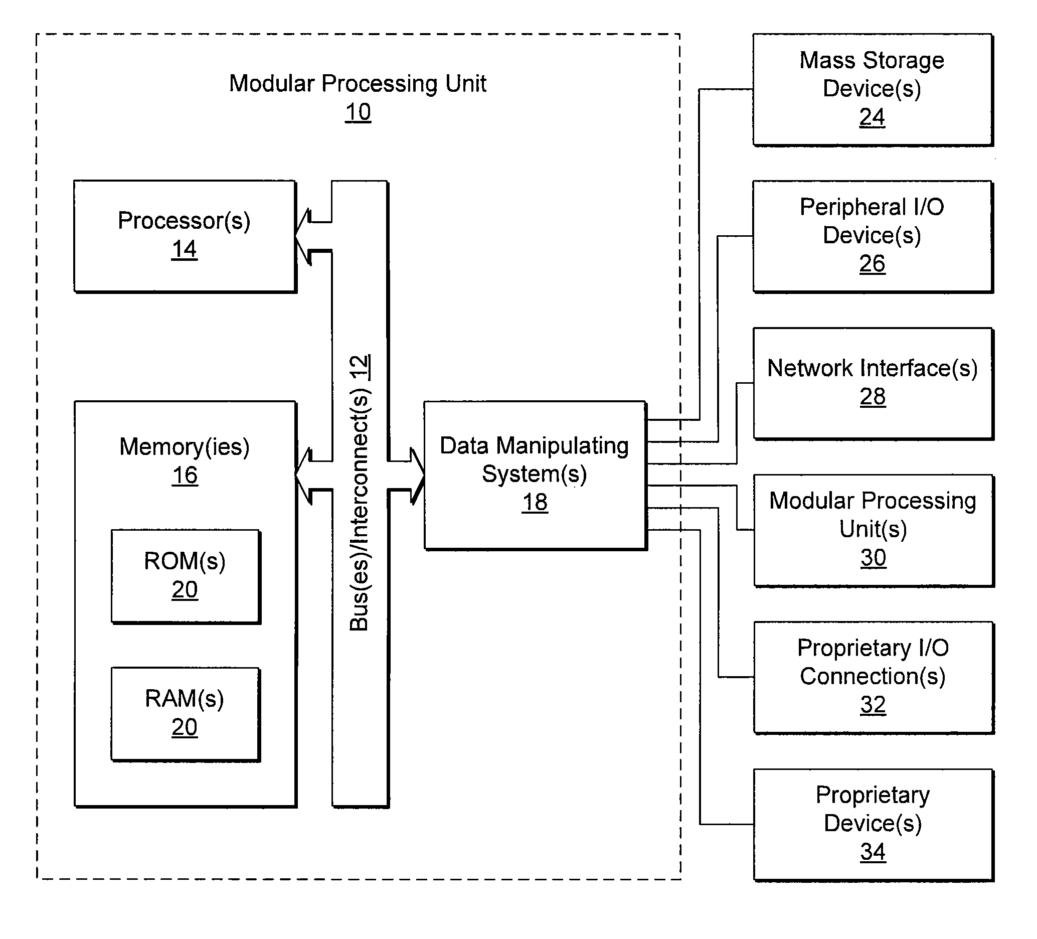
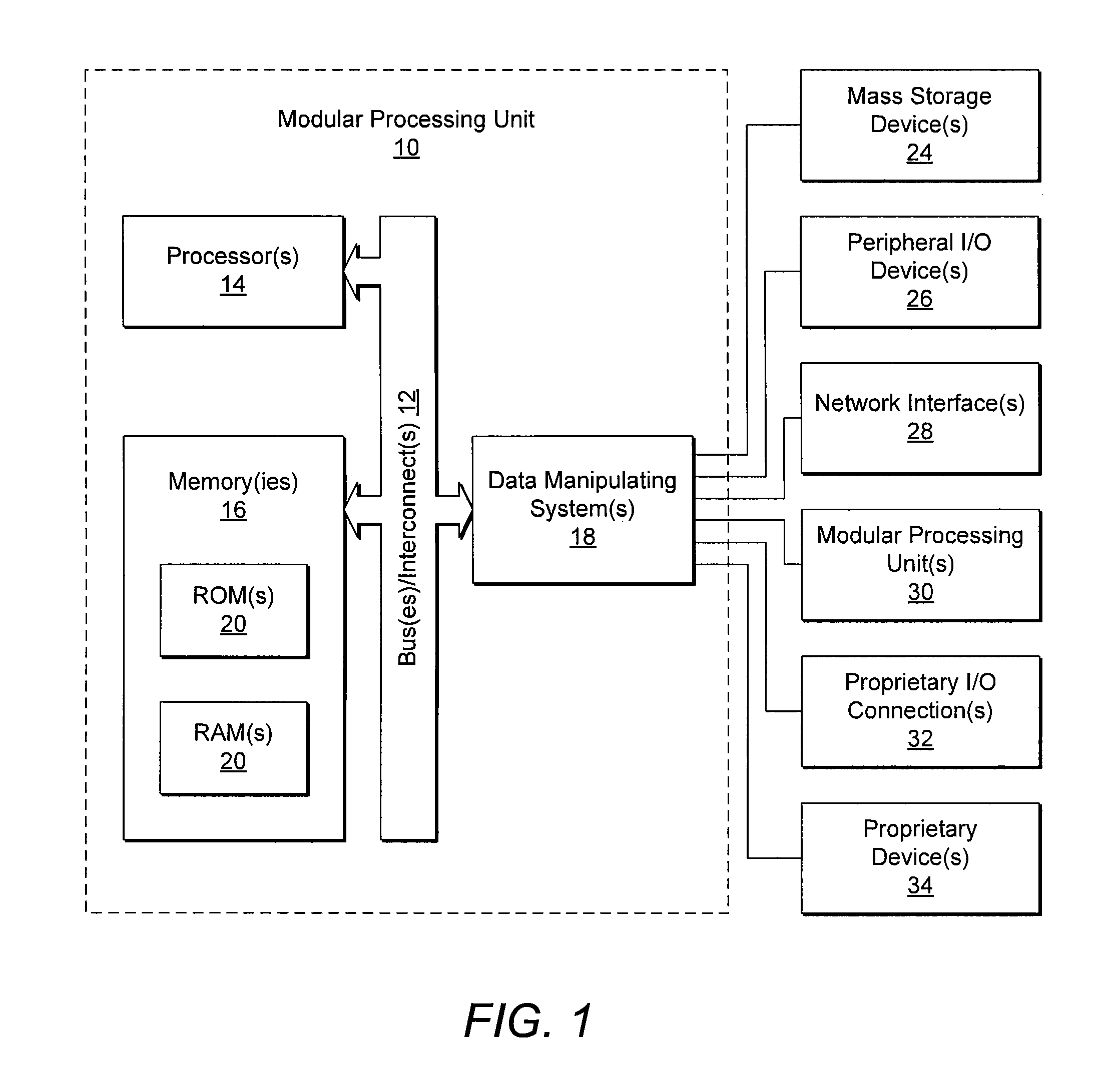
[0063]The present invention relates to electronic systems and components. In particular, the present invention relates to miniaturization techniques, systems, and apparatus relating to power supplies, memory, interconnections, and LEDs.

[0064]In the disclosure and in the claims, the term array may refer to any suitable arrangement that comprises a plurality of adjacent rows and a plurality of adjacent columns.

[0065]The following disclosure of the present invention is grouped into five subheadings, namely “Representative Operating Environment,”“Power Supplies,”“Memory,”“IC Connectors,” and “Logic Chip / LED Connection.” The utilization of the subheadings is for convenience of the reader only and is not to be construed as limiting in any sense.

Representative Operating Environment

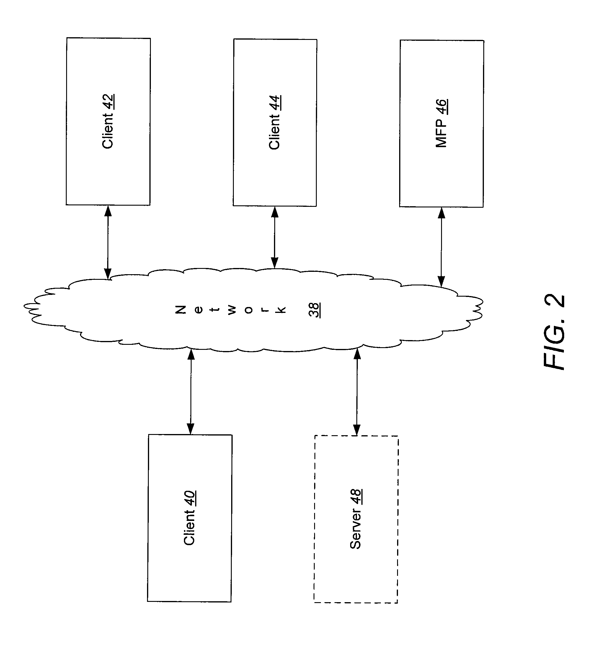
[0066]FIG. 1 and the corresponding discussion are intended to provide a general description of a suitable operating environment in accordance with embodiments of the present invention. As will be further discusse...


PUM


Abstract

Miniaturization techniques, systems, and apparatus relating to power supplies, memory, interconnections, and LEDS are described herein. Specifically, some aspects of the invention relate to techniques for miniaturization of power supplies. Other aspects relate to systems and methods for optimizing memory performance in a computer device or system. Still further, some aspects relate to systems and methods for miniaturizing and optimizing memory layout on a circuit board. Other aspects relate to systems and methods for attaching an integrated circuit, which comprises an array of pins, to a circuit board through the use of an adaptor that comprises a BGA, and which is configured to electrically and physically attach to the circuit board. Furthermore, some aspects relate to systems and methods for achieving activation of at least one multi-color LED, such as a bi-color or tri-color LED, using multiple electrical ground outputs or signals intended to activate only a single unicolor LED.

Description

CROSS-REFERENCE TO RELATED APPLICATIONS[0001]This application claims the benefit of the following provisional applications: U.S. Provisional Application No. 61 / 352,359, filed Jun. 7, 2010, entitled “MINITURIZED POWER SUPPLY;” U.S. Provisional Application No. 61 / 352,349, filed Jun. 7, 2010, entitled “SYSTEMS AND METHODS FOR OPTIMIZING MEMORY PERFORMANCE;” U.S. Provisional Application No. 61 / 352,369, filed Jun. 7, 2010, entitled “SYSTEMS AND METHODS FOR PROVIDING A PIN GRID ARRAY TO BALL GRID ARRAY ADAPTOR;” and U.S. Provisional Application No. 61 / 352,378, filed Jun. 7, 2010, entitled “SYSTEMS AND METHODS FOR ACTIVATING MULTI-COLOR LIGHT EMITTING DIODES; the entire disclosures of all of the applications are hereby incorporated by reference.BACKGROUND OF THE INVENTION[0002]1. Field of the Invention[0003]The present invention relates to electronic systems and components. In particular, the present invention relates to miniaturization techniques, systems, and apparatus relating to power ...

Claims


Application Information

Patent Timeline
Patent Type & Authority Applications(United States)
IPC IPC(8): G11C5/02H05B37/02H05K7/00H01R31/06
CPCG06F1/10G06F1/183G06F1/188G11C5/14H05B37/0254G11C5/02G06F1/26H05K1/113H05K1/181H05K2201/10545H05B47/18Y02P70/50
Inventor SULLIVAN, JASON A.ABDOUCH, CHARLES
Owner ATD VENTURES
Why Eureka
Try Eureka