Electrochromic unit and display device using the same

a technology applied in the field of electrochromic units and display devices, can solve the problems of not being able to switch to display 2d images, environmental protection and toxicity, and the manufacturing process is very complicated

Inactive Publication Date: 2012-01-26
J TOUCH CORPORATION
View PDF6 Cites 12 Cited by
  • Summary
  • Abstract
  • Description
  • Claims
  • Application Information

AI Technical Summary

Benefits of technology

[0020]Therefore, a 3D image is divided into a left-eye image and right-eye image when the image display unit is switched from displaying 2D images to 3D images. Now, the transparent conductive elements are electrically conducted, such that the color of the electrochromic layers is changed from a transparent area into a dark light shield area according to the arrangement of the electrochromic units with an interval apart from each other. The electrochromic unit produces a plurality of light shield areas arranged with an interval apart and divides th

Problems solved by technology

However, present existing stereo image display devices can display 3D images only, but they cannot be switched to display 2D images and 3D images primarily because images passed through the lenticular lens or barrier combined with a general display device will be divided into a left-eye image and a right-eye image, unless an external 3D image display module is used for attaching into the display device, and the external 3D image display module can be removed from the device when there is no need of displaying 3D images.
Although the organic material provides a faster reaction, it has issues of environment protection and toxicity.
In addition, the transparent electrode layer and electrochromic material layer of the parallax barrier device are grid patterned, and whose manufacturing process requires a precise alignm

Method used


Image

  • Electrochromic unit and display device using the same
  • Electrochromic unit and display device using the same
  • Electrochromic unit and display device using the same

Examples


Embodiment Construction

[0043]The technical characteristics and effects of the present invention will be apparent with the detailed description of preferred embodiment together with the illustration of related drawings as follows.

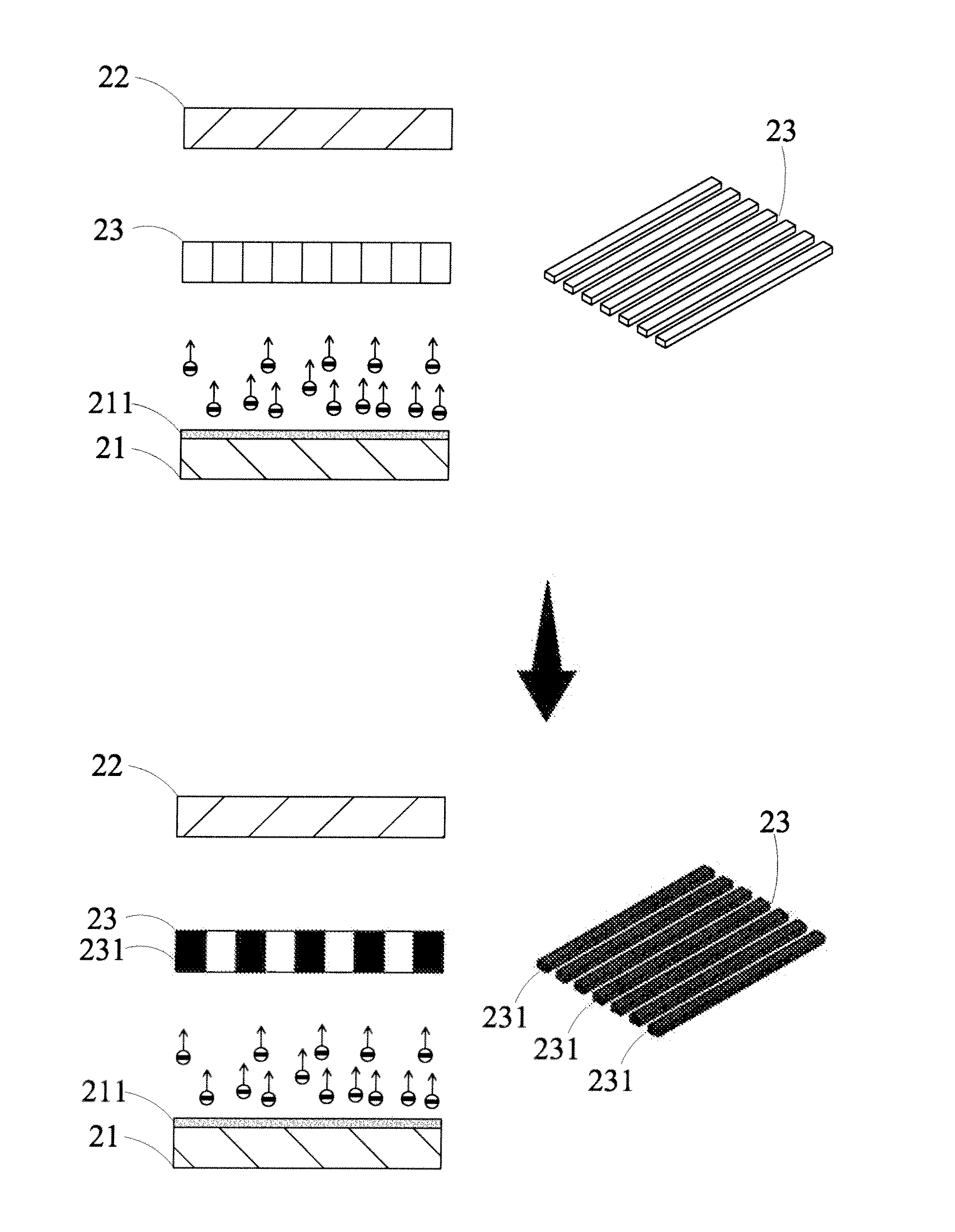
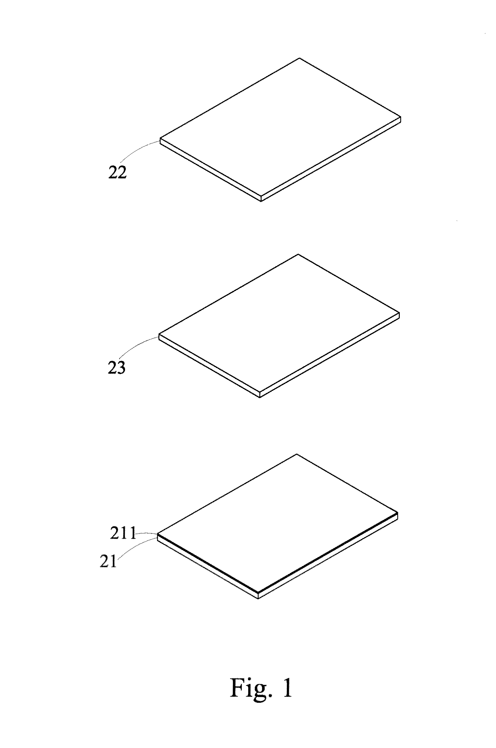
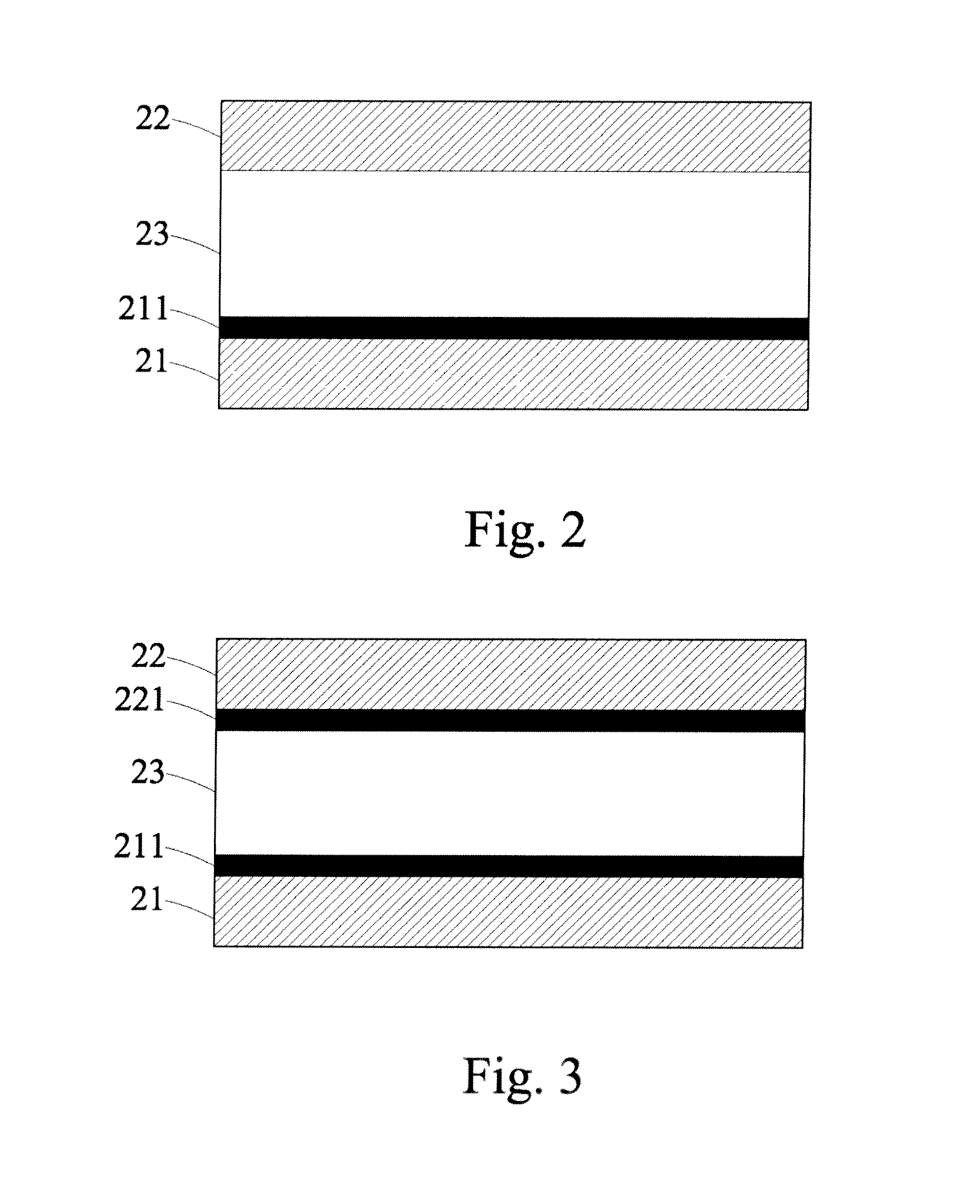
[0044]With reference to FIGS. 1 to 3 for an exploded view of an electrochromic unit 2 a first schematic view of a transparent conductive element and a second schematic view of a transparent conductive element in accordance with a first preferred embodiment of the present invention respectively, the electrochromic unit 2 comprises a first transparent substrate 21, a second transparent substrate 22, an electrochromic layer 23 formed between the first and the second transparent substrates 21, 22, and a first transparent conductive element 211, wherein the first transparent conductive element 211 can be installed on a surface of the first transparent substrate 21 (as shown in FIG. 1) or on a surface of the second transparent substrate 22 (as shown in FIG. 2), or the transparent conduc...


PUM


Abstract

In an electrochromic unit and a display device using the electrochromic unit, the electrochromic unit includes a first transparent substrate, a second transparent substrate, and a transparent conductive element and an electrochromic layer formed between the substrates, and electrons are used for changing the valence of ions of an electrochromic material, such that a reduction is resulted by supplying electrons and an oxidation is resulted by removing electrons to change colors, and the electrochromic coloration rate is quicker and more uniform and the driving voltage is smaller than those of the present existing electrochromic materials. A coloration/decoloration electrochromism can be achieved in a different way than the method of applying the dual addition and dual removal of ions and electrons in organic/inorganic electrochromic material.

Description

CROSS-REFERENCE TO RELATED APPLICATIONS[0001]This non-provisional application claims priority under 35 U.S.C. §119(a) on Patent Application No(s). 099124255 filed in Taiwan, R.O.C. on Jul. 22, 2010, the entire contents of which are hereby incorporated by reference.[0002]This non-provisional application claims priority under 35 U.S.C. §119(a) on Patent Application No(s). 201010287041.5 filed in China on Sep. 17, 2010, the entire contents of which are hereby incorporated by reference.BACKGROUND OF THE INVENTION[0003]1. Field of the Invention[0004]The present invention relates to a display device, and more particularly to an electrochromic unit and a display device using the electrochromic unit.[0005]2. Description of the Related Art[0006]The principle of present well-known stereo image display technologies adopts a binocular disparity for receiving different images from both left and right eyes of a user respectively, and finally the user's brain merges the images into a stereo image....

Claims


Application Information

Patent Timeline
IPC IPC(8): G02F1/153B82B1/00B82Y99/00G02B30/27G02B30/30
CPCG02F1/15G02F2201/44G02B27/2214G02B30/27G02F1/1524G02F1/161G02B30/30G02F1/163G02F1/157
Inventor YEH, YU-CHOUWANG, CHAO-YIYEH, TSUNG-HER
Owner J TOUCH CORPORATION
Why Eureka
Try Eureka