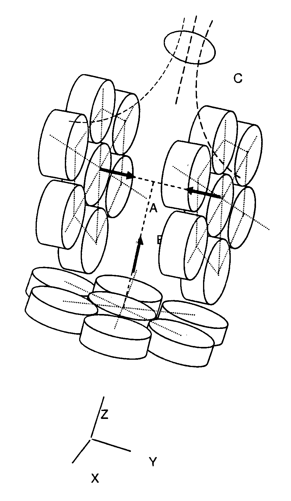
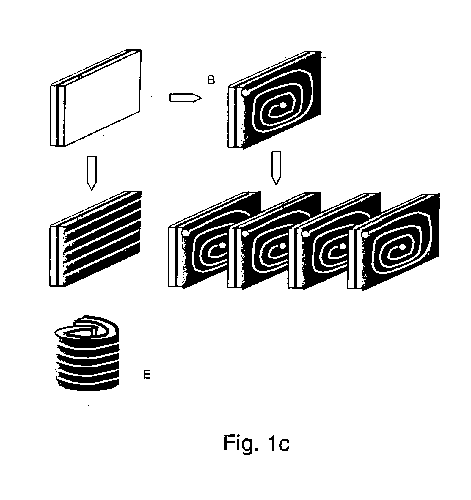
[0013]An advantageous approach is, therefore, provided according to the first aspect of the present invention in which essentially “concentric” support surfaces are provided as one continuous
support surface in the general form of a spiral nested in a concentric manner, preferably coated with a single HTS thin film layer with lithographed defined current paths. Conventional conductor can be paths on the
support surface, such that the number of
Ampere-turns of a field creating module are increased in proportion to the number of concentric
layers. This has two advantages over separate concentrically nested support surfaces. The first
advantage is that the number of non-superconducting connections between concentrically supported coated
layers is reduced for a given total number of
Ampere-turns, so allowing the defined current path to act as a
continuous current path in a
superconducting material, thereby avoiding heat production within a module. The second
advantage of using a general spiral form of the defined current path, such that the defined current path is now continuous and in the general spiral geometry, which replicates multiple concentric surfaces, is that the number of Ampere-turns is greatly increased in a compact arrangement, thus facilitating manufacture and decreasing the cost of field sources.
[0016]Therefore, an improvement in the performance of magnet modules intended for MRI magnet arrays is provided by combining in each module a primary substantial field source based on limited lengths of continuous coated conductor in radial multi-turn geometry, with a secondary lesser field source using defined current paths on a coated, closed surface. The secondary source adapts the field of the
primary source so that, when combined, a plurality of such module primary sources in arrays provides improved array MRI
field uniformity.
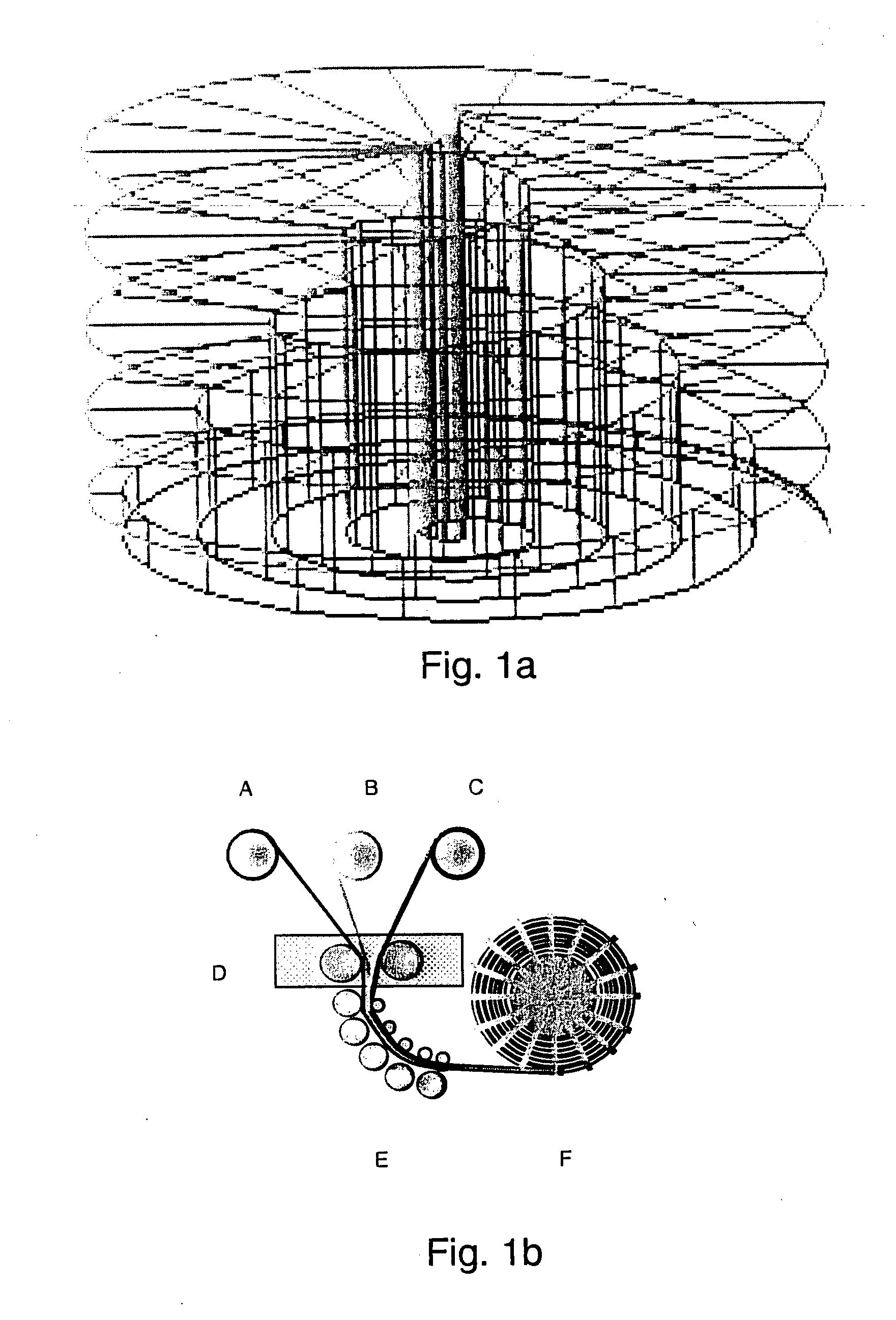
[0017]The
secondary field source allows for the alteration of the
principal direction of magnetic field of each PCMM relative to the geometry of the PCMM, by variation of applied currents. This is an
advantage in a MRI magnet formed from arrays of PCMM in that the MRI field can be adapted in use, for example to change the MRI field profile against experimental needs or to compensate for changes in magnetic environment caused such as by introducing patients or their support equipment. Importantly, the
secondary field source is close to the origin of the
primary field source. In operation, this means that projected fields are corrected (“at source”) without introduction of higher order field derivatives, (field perturbations) which might give rise to additional distortions of the MRI field. In essence, the use of duel field sources in PCMM means a MRI magnetic can be adapted in respect of the MRI field without adding additional undesirable distortions of the MRI field, as opposed to
current practice using LTS magnets whereby
primary field errors are shimmed to a limited degree by shims close to the MRI region, which usually cause high order field perturbations when correcting low order
primary field errors.
[0018]One further advantage of modules in a preferred embodiment is that sealed units of factory tested capability can be manufactured wherein handling uncertainties of the preferred delicate HTS conductor are avoided during magnet
assembly. Note, LTS
Niobium tin conductors, with similar mechanical properties to HTS thin films, are shipped to magnet manufactures as component composites, wound, and then reacted by the magnet manufacturer to form the LTS material in-situ in the magnet, thus avoid handling uncertainties. HTS thin films cannot be organised in this way because of complicated phase
chemistry. The modular aspect of the field delivery means that limited volumes of HTS can be accommodated using existing and foreseeable thin film deposition methods constrained to deliver high quality material on a
batch production basis. A further point of note concerning
modularity of field sources involves magnet arrays that make possible LTS
niobium tin whole body MRI magnets that could deliver higher magnetic fields than generally available with current LTS
engineering, depending on the concept of reaction of composite conductor in discrete-units.
[0020]A preferred method to assemble modules is via a
low resistance network of
bus bars. Such a
system would be cryo-resistive, as distinct from having persistent mode operation. However, because the HTS conductor operates under a regime of intermediate cryogenic temperatures, the
bus bar network, including interconnects, would be a few ohms in resistance, enabling the use of power supplies delivering intermediate currents at
low voltage and with high stability. The array of modules behaves as a cold
electromagnet. The dimensions of the current path remain constant in use because the magnet operates using super-currents in the major part of the defined current paths, under controlled
refrigeration to provide a constant temperature. This has the advantage over conventional electromagnets that the field profile of the combine field of modules remains constant over time during operation. There is no drift with time in
field uniformity in the MRI region.

