Plasma processing apparatus and plasma processing method

a plasma processing apparatus and plasma technology, applied in the field of plasma processing apparatus and inductively coupled plasma processing methods, can solve the problems of reducing the rf power to be supplied to the plasma load as much as the loss, the plasma density on the substrate is not sufficiently uniform for most plasma processes, and the loss of rf power within the high frequency power supply unit is great, so as to achieve the effect of reducing the loss of primary current, increasing the apparent load resistance of the primary coil, and ensuring the distribution

Active Publication Date: 2012-03-29
TOKYO ELECTRON LTD
View PDF10 Cites 13 Cited by
  • Summary
  • Abstract
  • Description
  • Claims
  • Application Information

AI Technical Summary

Benefits of technology

[0013]In view of the foregoing, the present disclosure provides an inductively coupled plasma processing apparatus and a plasma processing method capable of reducing a RF power loss within a high frequency power supply unit (particularly, a matching unit) and enhancing a plasma generation efficiency.
[0014]Further, the present disclosure provides an inductively coupled plasma processing apparatus capable of enhancing a plasma generation efficiency as described above and simplifying a matching unit.
[0018]As described above, each secondary current may flow through each antenna within each secondary circuit. As a result, inductively coupled plasma may be generated at a plasma generation space corresponding to each antenna by an electronic energy radiated from each antenna to a processing gas within a processing chamber via a dielectric window. Thus, the plasma generated at the plasma generation space within the processing chamber may be diffused in all directions, so that in a vicinity of a substrate holder, i.e. on a substrate, a plasma density may become uniformized. At this time, by setting or variably controlling an electrostatic capacitance of a capacitor provided in each secondary circuit to be an appropriate value, it is possible to control balance between the secondary currents flowing through the multiple antennas. Accordingly, it is possible to readily control a plasma density distribution on the substrate.
[0019]Further, in the high frequency power supply unit, the multiple antennas may be electrically connected to the primary coil via respective secondary coils. Therefore, an apparent load resistance of the primary coil may be increased. Thus, the primary current may be decreased and a RF power loss in the high frequency power supply unit can be reduced. Accordingly, a RF power to be supplied to a plasma load becomes increased, and a plasma generation efficiency becomes enhanced.
[0020]In accordance with a plasma processing apparatus or a plasma processing method of the present disclosure, with the above-described configuration and operation, it is possible to enhance a plasma generation efficiency by reducing a power loss within a high frequency power supply unit (particularly, a matching unit), and also possible to simplify the matching unit.

Problems solved by technology

However, only with a conventional RF antenna, the plasma density on a substrate is not sufficiently uniform for most plasma processes.
As for an inductively coupled plasma processing apparatus, it is also one of the most important issues to improve uniformity of a plasma density on a substrate since a uniformity / reproducibility and a production yield of a plasma process depend on the plasma uniformity.
Therefore, there is a great loss of a RF power within the high frequency power supply unit (particularly, the matching unit), and the RF power to be supplied to the plasma load is decreased as much as the loss.

Method used


Image

  • Plasma processing apparatus and plasma processing method
  • Plasma processing apparatus and plasma processing method
  • Plasma processing apparatus and plasma processing method

Examples


embodiment or modification example

Another Embodiment or Modification Example

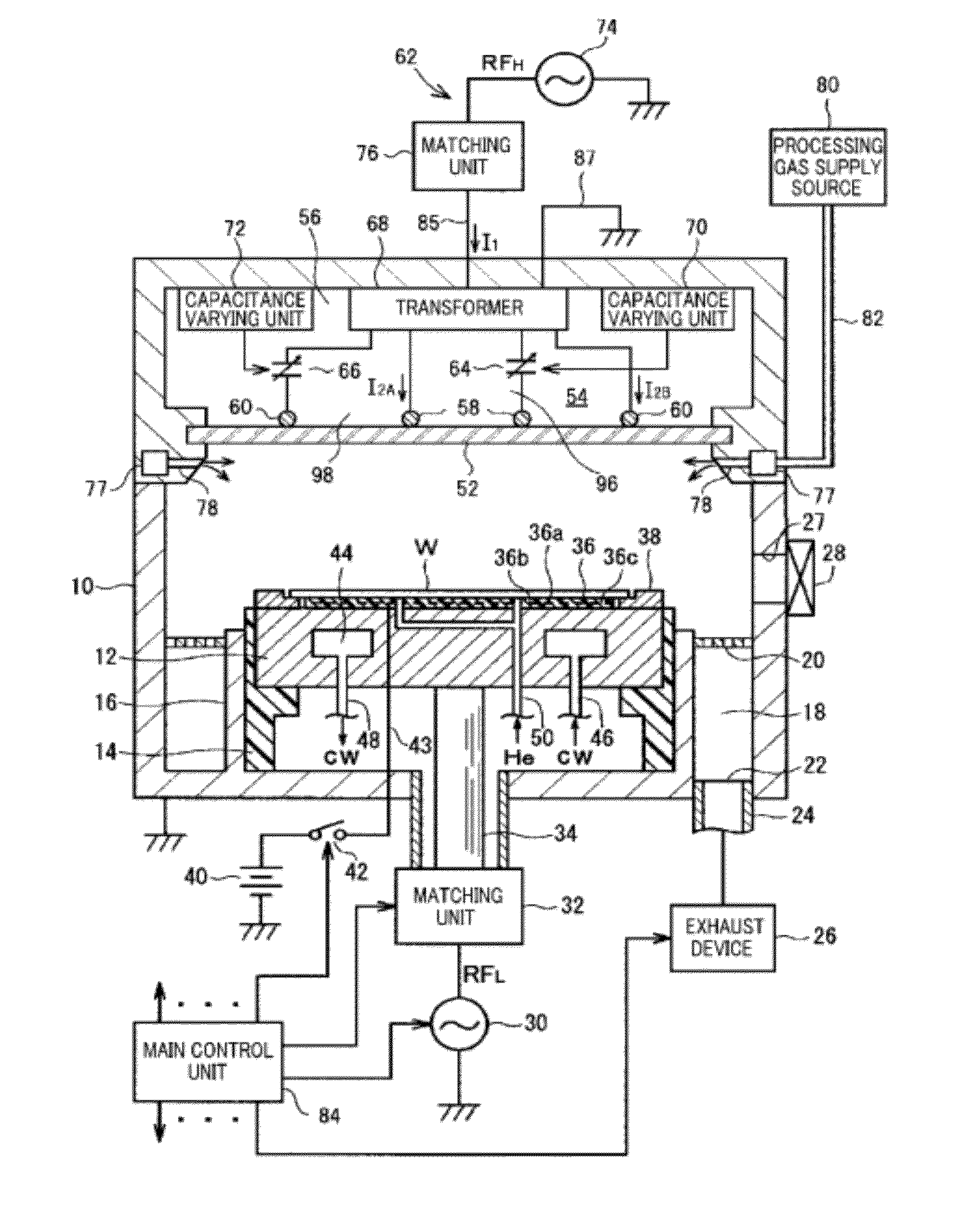
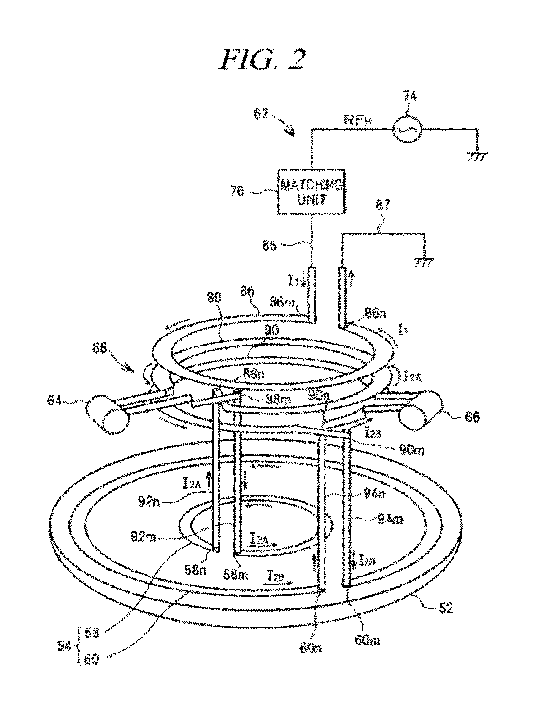
[0128]In the inductively coupled plasma processing apparatus (FIGS. 1 and 2) of the above-described embodiment, the transformer 68 is provided within the antenna chamber 56. However, the transformer 68 may be provided outside the antenna chamber 56. Further, any arrangements or directions of the primary coils 86 and / or the secondary coils 88 and 90 can be selected.

[0129]In the inductively coupled plasma processing apparatus of the above-described embodiment, the capacitors 64 (100) and 66 (102) are provided at all the secondary circuits 96 and 98 provided between the coaxial antenna group 54 and the transformer 68. However, by way of example, each of the primary coil 86 and the secondary coils 88 and 90 of the transformer 68 may be coiled multiple times, and a tap switch may be provided to the secondary coils 88 and 90 (i.e. the secondary currents I2A and I2B are controlled by the tap switch). With this configuration, the capacitors can be o...


PUM

PropertyMeasurementUnit
impedanceaaaaaaaaaa
frequencyaaaaaaaaaa
dielectricaaaaaaaaaa

Abstract

There is provided an inductively coupled plasma processing apparatus capable of reducing a RF power loss within a high frequency power supply unit (particularly, a matching unit) and capable of enhancing a plasma generation efficiency. In this inductively coupled plasma processing apparatus, a multiple number of closed-loop secondary circuits 96, 98 independent from each other are formed between a coaxial antenna group 54 and a transformer 68. Further, by varying electrostatic capacitances of variable capacitors 64 and 66, secondary currents I2A and I2B flowing through an inner antenna 58 and an outer antenna 60, respectively, of the coaxial antenna group 54 are independently controlled. Accordingly, it is possible to readily control a plasma density distribution on a semiconductor wafer W in a diametrical direction.

Description

CROSS-REFERENCE TO RELATED APPLICATION[0001]This application claims the benefit of Japanese Patent Application No. 2010-217271 filed on Sep. 28, 2010, and U.S. Provisional Application Ser. No. 61 / 391,946 filed on Oct. 11, 2010, the entire disclosures of which are incorporated herein by reference.FIELD OF THE INVENTION[0002]The present disclosure relates to a technique for performing a plasma process on a target substrate, and more particularly, to an inductively coupled plasma processing apparatus and an inductively coupled plasma processing method.BACKGROUND OF THE INVENTION[0003]In a manufacturing process of a semiconductor device or a FPD (Flat Panel Display), plasma is used to perform a process, such as etching, deposition, oxidation or sputtering, so as to perform a good reaction of a processing gas at a relatively low temperature. Conventionally, plasma generated by a high frequency electric discharge in MHz frequency band has been used in this kind of plasma process. The plas...

Claims


Application Information

Patent Timeline
Patent Type & Authority Applications(United States)
IPC IPC(8): C23F1/00C23C16/448H05H1/46C23F1/08
CPCH01J37/321H01J37/32174H01J37/3211H01J37/32183
Inventor YAMAZAWA, YOHEI
Owner TOKYO ELECTRON LTD
Why Eureka
Try Eureka