Touch panel

a technology of touch panel and touch plate, applied in the field of touch panel, can solve the problems of easy defective products and difficulty in producing thinner electronic products, and achieve the effect of improving adhesiveness

Inactive Publication Date: 2012-03-29
CATCHER TECH
View PDF5 Cites 26 Cited by
  • Summary
  • Abstract
  • Description
  • Claims
  • Application Information

AI Technical Summary

Benefits of technology

[0014](4) The barrier layer according to the present invention can improve adhesiveness and etching property of the s

Problems solved by technology

However, the manufacturing process of the touch panel and the display panel that have multi assemblies therebetween will consume more raw materials; furthermore, the practice manufacturing procedure of the touch panel comprises the steps of accomplishing the process of forming ea

Method used


Image

  • Touch panel
  • Touch panel
  • Touch panel

Examples


Embodiment Construction

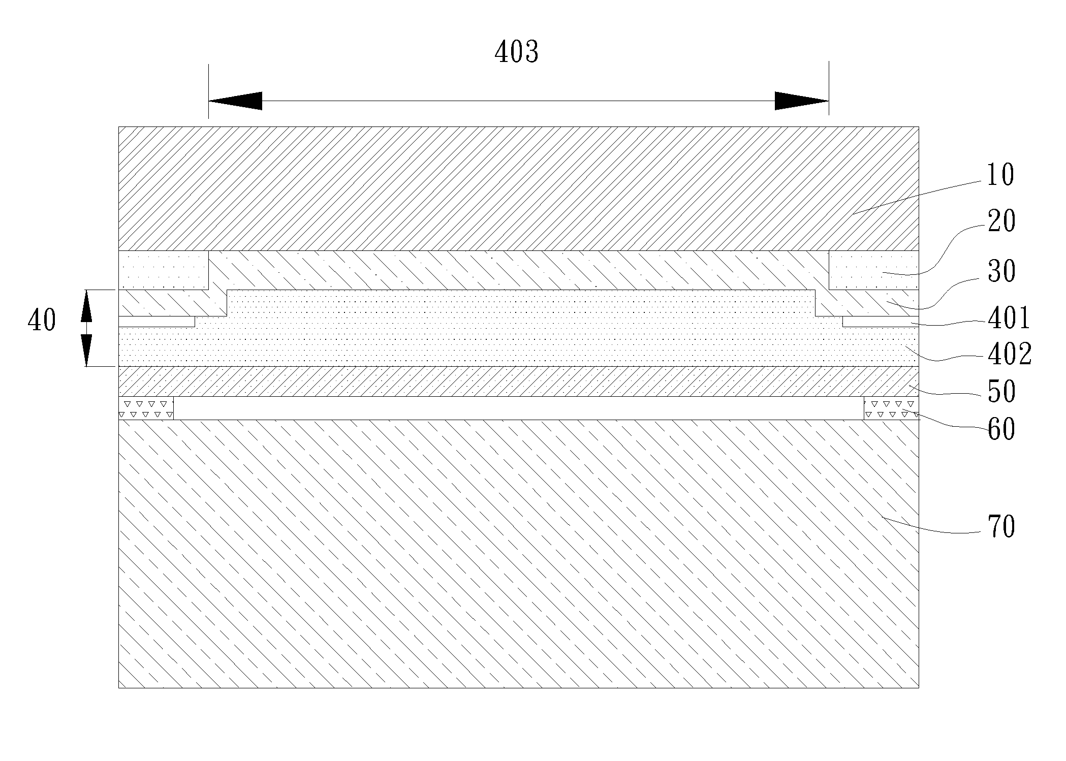
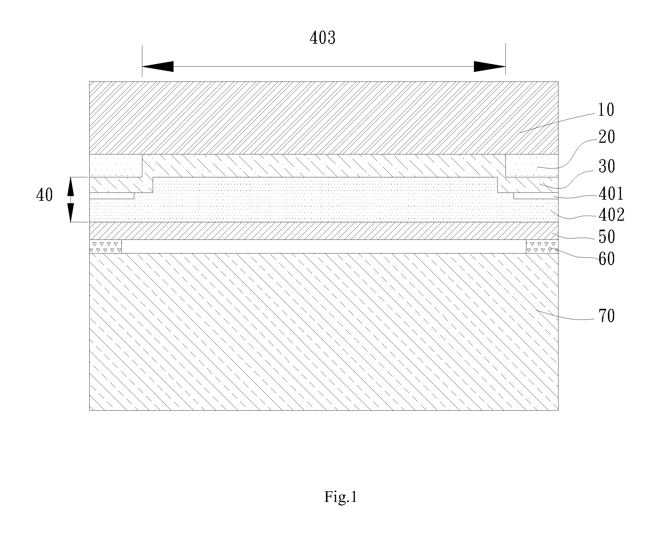
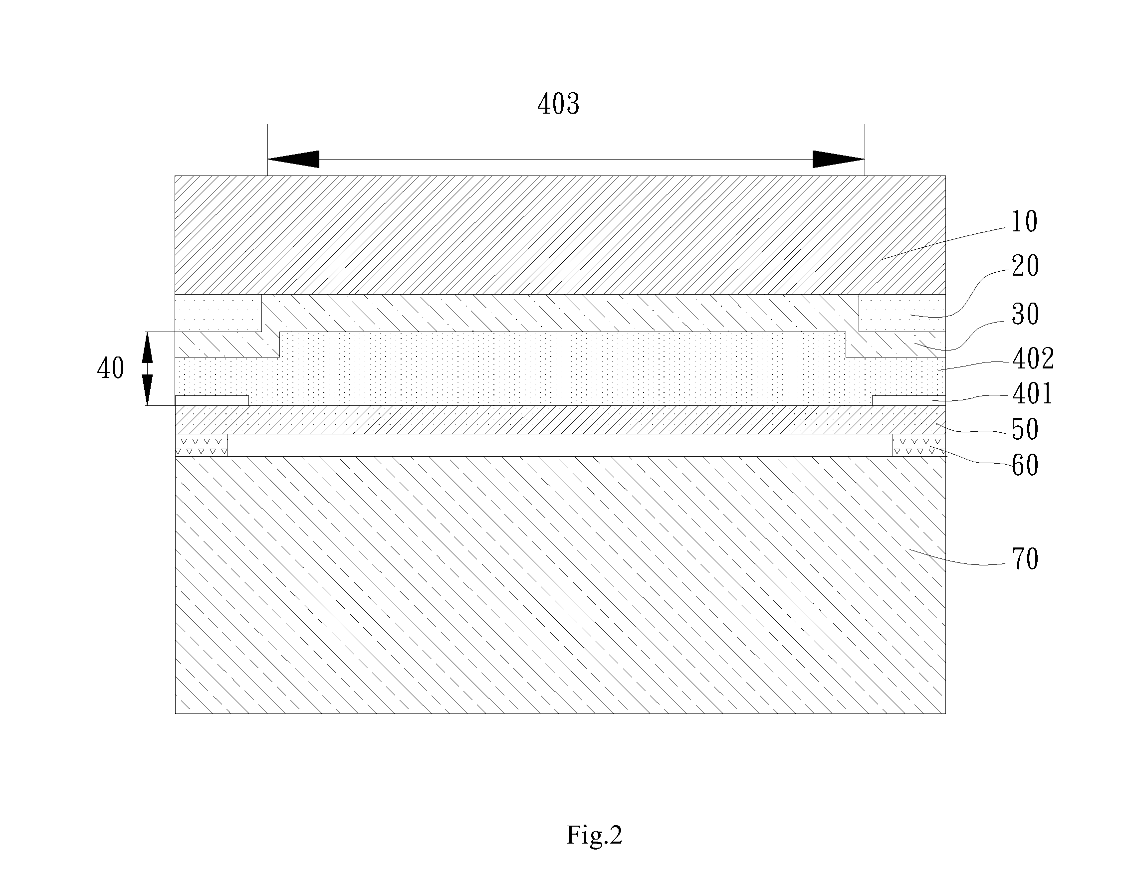
[0019]Please refer to FIG. 1 which is a cross-sectional schematic diagram showing a touch panel according to a first preferred embodiment of the present invention. As shown in FIG. 1, the touch panel comprises a substrate 10, a mask layer 20, a sensing circuit layer 40 and a barrier layer 30. The substrate 10 could be glass, which has a top surface and a bottom surface. The mask layer 20 is disposed around the bottom surface of the substrate 10, and the mask layer 20 is black matrix or other coating layer with shielding effect, such as metallic layer or organic layer. In addition, the sensing circuit layer 40 is disposed on the substrate 10 and the sensing circuit layer 40 is located on the same side of the substrate as the mask layer 20, such that a surrounding area of the sensing circuit layer 40 is shielded by the mask layer 20. Except for the area shielding by the mask layer 20, the sensing circuit layer 40 further exposes externally a sensing area 403. Furthermore, the present ...


PUM


Abstract

A touch panel, which contains a substrate, a mask layer, a sensing circuit layer and a barrier layer, is disclosed. The mask layer is disposed around the bottom surface of the substrate. The sensing circuit layer is located on the same side of the substrate with the mask layer, and the surrounding area of the sensing circuit layer is shielded by the mask layer. In addition, the area of the sensing circuit layer exposed from the mask layer is defined as a sensing region. Furthermore, the barrier layer is disposed between the substrate and the sensing circuit layer and between the mask layer and the sensing circuit layer. Concurrently, the barrier layer further provides separation between the mask layer and the sensing circuit layer. The barrier layer has a transparent appearance. Particularly, the barrier layer is provided for changing optical refraction and harmonizing optical reflection index and transmittance.

Description

FIELD OF THE INVENTION [0001]The present invention relates to a touch panel, and more particularly to a touch panel which comprises a barrier layer disposed between the mask layer and the sensing circuit layer.BACKGROUND OF THE INVENTION [0002]Currently, the touch panel has been quite popular in use, and it is quite convenient for the users to proceed the inputs or other operations by merely click the figures and texts shown in the panel with their fingers or pen-like objects.[0003]However, the manufacturing process of the touch panel and the display panel that have multi assemblies therebetween will consume more raw materials; furthermore, the practice manufacturing procedure of the touch panel comprises the steps of accomplishing the process of forming each individual structure layer first, and then integrating all of these individual layers into an unity. As a result, the defective products may occur easily due to the foregoing complicated assembly procedure. In addition, the thi...

Claims


Application Information

Patent Timeline
IPC IPC(8): G06F3/041
CPCG06F3/0412G06F2203/04107G06F2203/04103G06F3/044G06F3/0443
Inventor LEE, CHIEN-WEICHEN, YAN-WEILIN, CHIH-LUNG
Owner CATCHER TECH
Why Eureka
Try Eureka