
Organic electronic device and method for producing the same

a technology of electronic devices and electronic components, applied in the direction of solid-state devices, semiconductor devices, thermoelectric devices, etc., can solve the problems of difficult electrical charge injection and element driving, and achieve the effects of improving hydrophilicity/hydrophobicity, film strength and flexibility, and high power efficiency and long li

Active Publication Date: 2012-04-19
DAI NIPPON PRINTING CO LTD
View PDF6 Cites 26 Cited by
  • Summary
  • Abstract
  • Description
  • Claims
  • Application Information

AI Technical Summary

Benefits of technology

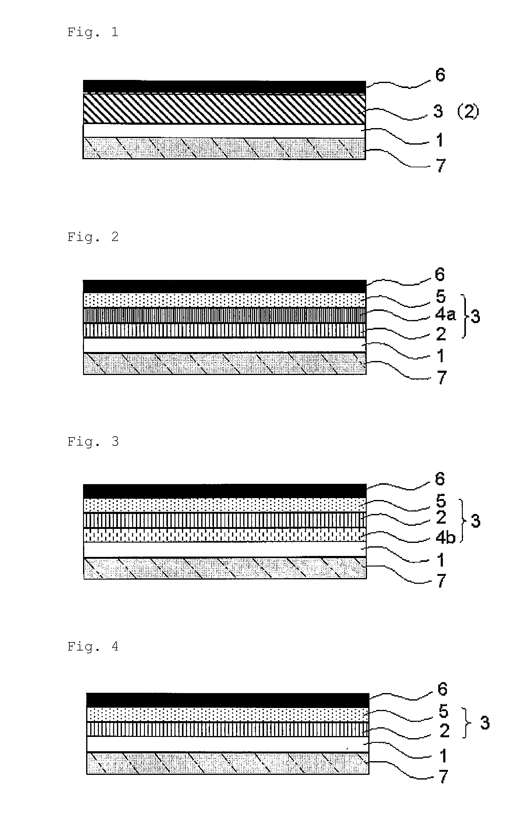
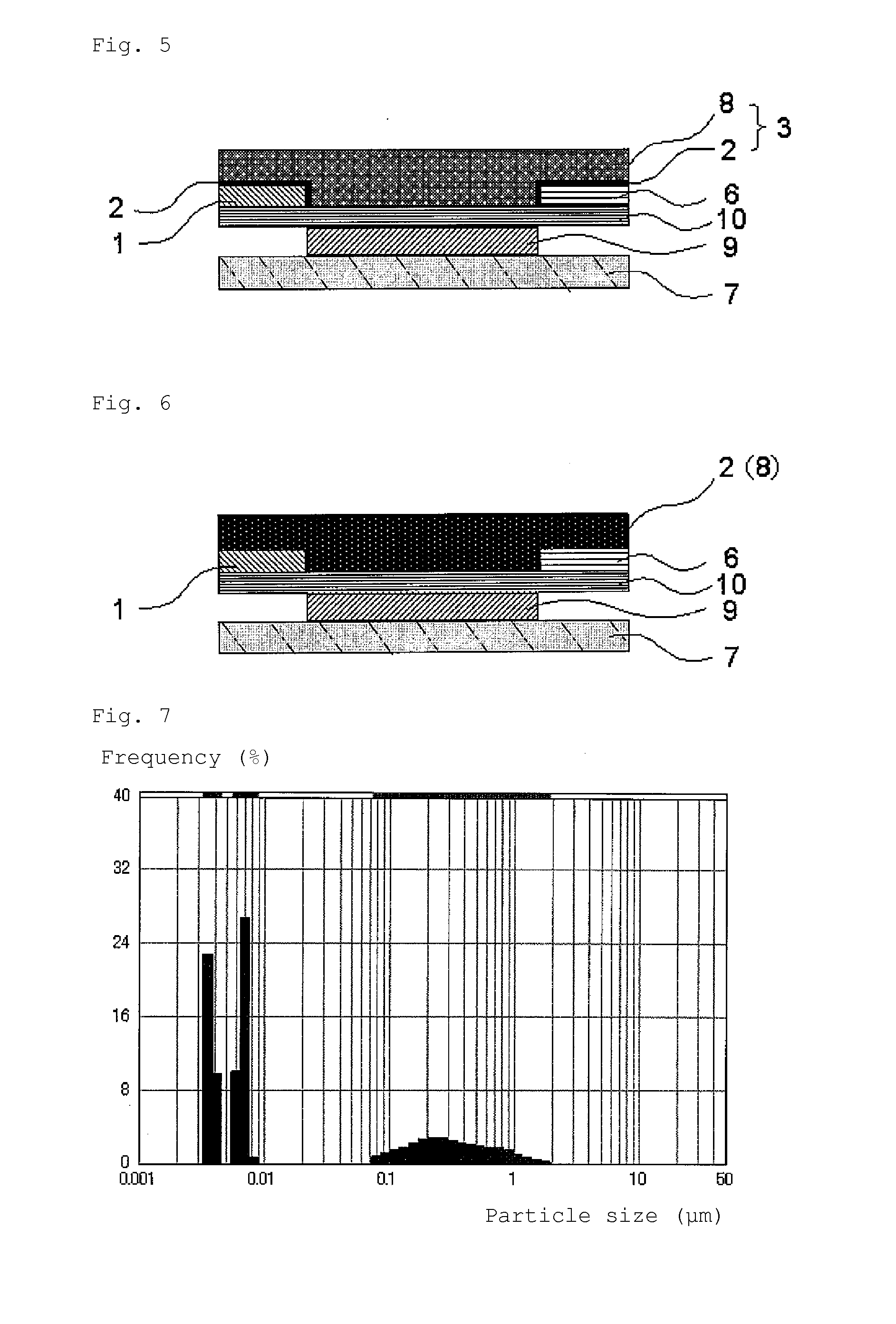
[0063]The organic electronic device of the invention, comprising a hole injecting layer and / or hole transporting layer containing metal oxide clusters that include at least one metal element selected from among elements of Group 5, Group 6 or Groups 8-10 of the Periodic Table, wherein the metal oxide clusters are chemically synthesized polyoxometalates, allows devices with low-voltage driving, high power efficiency and long lifetime to be realized.
[0064]In the organic electronic device of the invention, by using metal oxide clusters having not only a single valency state which is the valency of the metal element that is generally considered stable, but also having stable coexistence of metal elements with different valency states that are considered unstable, and adding an organic compound with a hole injection / transport property to the metal oxide clusters, it is possible to improve the hydrophilicity / hydrophobicity, the hole transport property or the coating film formability, film quality, film strength and flexibility, and to impart functionality such as adhesiveness, thus facilitating multifunctional modification of the hole injecting layer and / or hole transporting layer and increasing the function of the element.
[0065]In the organic electronic device of the invention, it is preferred to use not only metal oxide clusters composing the hole injecting layer alone, but also a hole-transporting material in which an organic compound with a hole transport property is able to stably dissolve, disperse or mix with the metal oxide clusters, in order to allow easy formation of a smooth hole injecting layer, and this can further reduce the driving voltage or improve the driving lifetime of the element.
[0066]It is also preferred because the hole injecting material and / or hole transporting material in the organic electronic device of the invention can easily adopt a stable fluid material state, so that it is possible to form the hole injecting layer and / or hole transporting layer by a coating method and facilitate the production process, while also minimizing shorts and allowing production yield to be increased and a long lifetime to be achieved.
[0067]In the organic electronic device of the invention, the organic functional layer may be one that has been formed by a coating method on the hole injecting layer and / or hole transporting layer. The hole injecting layer and / or hole transporting layer of the invention will occasionally be insoluble in the solvent used for the solution, after it has been formed by a coating method, in which case the organic functional layer may be laminated by a coating method.
[0068]As mentioned above, the organic electronic device of the invention contains metal oxide clusters in the hole injecting layer and / or hole transporting layer, thereby improving the hole injection property, and yielding a film with excellent adhesiveness with adjacent electrodes and organic functional layers and high stability, such that a long element driving lifetime can be achieved. Furthermore, the organic electronic device of the invention differs from those using the inorganic compound molybdenum trioxide (MoO3), in that the metal oxide clusters uniformly dissolve in solvents, or form uniform dispersions or mixtures, thus allowing a uniform fluid material to be formed, and since thin-film formation can therefore be accomplished by a coating method, the production process is facilitated.

Problems solved by technology

In order to obtain high luminous efficiency in an organic EL element it is necessary to efficiently and rapidly supply electrical charges (holes and electrons) to the luminescent material acting as the luminescent center, but due to a high energy barrier between the anode or cathode and the organic functional layer, such as the luminescent layer, injection of electrical charges is not easily accomplished.
When organic semiconductor materials employed in such organic transistors are used, however, the charge injecting barrier with the source electrode or drain electrode has been large, causing problems with element driving.

Method used


Image

  • Organic electronic device and method for producing the same
  • Organic electronic device and method for producing the same
  • Organic electronic device and method for producing the same

Examples


synthesis example 1

Synthesis Method for Water-Soluble Mo154 Clusters 1

[0247]After placing a magnetic stirrer in a 100 mL round-bottomed flask, disodium molybdate (VI) dihydrate (3.04 g), distilled water (25 mL) and 35% hydrochloric acid (2.47 mL) were added. Next, sodium dithionite (0.15 g) was added and the mixture was stirred at room temperature for 24 hours. The mixture was then allowed to stand for 5 days and the precipitated dark blue solid was filtered out and rinsed with cold water. The dark blue oily matter was transferred to a sample bottle and dried in a desiccator, to obtain dark blue solid water-soluble molybdenum oxide clusters (hereunder referred to simply as “Mo clusters 1”) (1.46 g).

[0248]Successful synthesis of Mo clusters 1 was confirmed by Fourier transform infrared spectroscopy (FT-IR) and Raman spectroscopy.

[0249]In FT-IR, an FT-IR apparatus by Varian (FTS6000) was used for measurement by the KBr method. The intensity distribution at each wavelength was measured by FT-IR to analyz...

synthesis example 2

Synthesis Method for Water-Soluble Mo146 Clusters 2

[0253]After placing a magnetic stirrer in a 100 mL round-bottomed flask, disodium molybdate (VI) dihydrate (3.04 g), distilled water (25 mL), 35% hydrochloric acid (2.47 mL) and formic acid (1 mL) were added. Next, sodium dithionite (0.15 g) was added and the mixture was stirred at room temperature for 24 hours. The mixture was then allowed to stand for 5 days and the precipitated dark blue solid was filtered out and rinsed with cold water. The dark blue oil was transferred to a sample bottle and dried in a desiccator, to obtain dark blue solid water-soluble molybdenum oxide clusters (hereunder referred to simply as “Mo clusters 2”) (0.43 g). Absorption wavenumbers: νcm−1,1617, 974, 912, 820, 747, 632, 557.

example 1

[0273]The substrate used was prepared by coating a photosensitive resist onto the ITO anode of an ITO-attached glass panel (product of Sanyo Vacuum Industries Co., Ltd., ITO film thickness: 150 nm) and performing mask exposure, development and etching for strip pattern formation to obtain a pattern-formed ITO substrate, and this was subjected to ultrasonic cleaning with a neutral cleanser and ultrapure water in that order, and to UV ozone treatment.

[0274]Next, 0.04 g of Na15[MoVI126MoV28O462H14(H2O)70]0.5[MoVI124MoV28O457H14(H2O)68]0.5.400H2O clusters, as the aqueous polyoxometalate chemically synthesized in Synthesis Example 1 (also referred to as “Mo154 clusters” or “Mo clusters 1”) was dissolved in 10 g of distilled water to prepare a coating ink as a hole injecting layer-forming coating solution. The coating ink was used for coating by spin coating onto the cleaned anode to a dry hole injecting layer film thickness of 10 nm, to form a hole injecting layer coating film. After for...


PUM

PropertyMeasurementUnit
Nanoscale particle sizeaaaaaaaaaa
Timeaaaaaaaaaa
Timeaaaaaaaaaa

Abstract

There is provided an organic electronic device that can exhibit a long lifetime while having a facilitated production process. An organic electronic device and a method for producing it, wherein the organic electronic device comprises two or more electrodes facing each other on a substrate, and an organic functional layer that includes at least a hole injecting layer and / or a hole transporting layer situated between two electrodes, wherein the hole injecting layer and / or hole transporting layer is formed as a thin-film from a fluid material that comprises anionic metal oxide clusters that include at least one metal element selected from among elements of Group 5, Group 6 or Groups 8-10 of the Periodic Table, the metal oxide clusters being polyoxometalates, dissolved or uniformly dispersed or mixed in an aqueous solvent.

Description

TECHNICAL FIELD[0001]The present invention relates to an organic electronic device and a method for producing it, and particularly it relates to an organic electronic device and a method for producing it, which encompass a wide range of basic elements and uses such as organic luminescent devices including organic electroluminescence elements, or organic transistors, organic solar cells and the like, and also quantum dot light emitting elements having hole injecting transport layers, and oxide-based compound solar cells.BACKGROUND ART[0002]Organic electronic devices employing organic materials are expected to be developed for a wide range of basic elements and uses including organic electroluminescence elements (hereunder, “organic EL elements”), organic transistors and organic solar cells. In addition, “organic devices”, in the wider sense of having a hole injecting transporting layer, include quantum dot light emitting elements in which organic EL luminescent dopants are replaced w...

Claims


Application Information

Patent Timeline
IPC IPC(8): H01L51/52H01L51/56
CPCH01L51/0038H01L51/506H01L51/5088H01L51/0081H01L51/0085H01L51/0059H10K85/114H10K85/631H10K85/324H10K85/342H10K50/155H10K50/17H10K50/15
Inventor UENO, SHIGEHIROOKADA, MASATOKOMUKAI, MAKOTOASOU, MASATOMATSUHASHI, TAKESHIIKEDA, KAZUNARI
Owner DAI NIPPON PRINTING CO LTD
Learn More