Method for preparation of metal chalcogenide solar cells on complexly shaped surfaces

a solar cell and complex technology, applied in the direction of photovoltaic energy generation, coatings, semiconductor devices, etc., can solve the problems of increasing installation costs, and increasing the cost of solar cell modules

Inactive Publication Date: 2012-04-26
IMRA AMERICA
View PDF0 Cites 41 Cited by
  • Summary
  • Abstract
  • Description
  • Claims
  • Application Information

AI Technical Summary

Problems solved by technology

The remainder of the cost is associated with module installation and other fixed costs such as inverter installation and connecting the cells to the grid.
As the cost of solar cell modules continues to decrease, installation costs are poised to become greater than the module costs.
Two strategies were previously developed to deposit CIGS on these cylindrical surfaces, but each has drawbacks.
The disadvantage of this wrapping approach is the shear stress which occurs in the film.
CIGS is a ceramic material that is prone to cracking; the wrapping process can stress the film, reducing efficiency.
However, though electrochemical deposition can be used to deposit a conformal absorber layer, deposition of all of the necessary elements from a single electrochemical deposition bath is difficult because of the large difference in deposition potentials of copper, indium, gallium, and selenium.
While theoretically possible, no uniform deposition of CIGS from a single bath has been demonstrated.
With the exception of electrochemical deposition, all of the other methods that have been developed for depositing CIGS are line-of-sight techniques, which make them incompatible with deposition on complexly shaped surfaces.
Methods based on physical vapor

Method used


Image

  • Method for preparation of metal chalcogenide solar cells on complexly shaped surfaces
  • Method for preparation of metal chalcogenide solar cells on complexly shaped surfaces
  • Method for preparation of metal chalcogenide solar cells on complexly shaped surfaces

Examples


Embodiment Construction

[0014]In the present application, the following terms are defined as below, unless indicated otherwise.

[0015]“Nanoparticles” refers to particles having a size ranging from about 1 nanometer (nm) to 100 micrometer (μ) in at least one dimension.

[0016]“Surface-charged” particles refer to nanopartieles having a shield of charges at the interface between the particle surface and the surrounding liquid medium.

[0017]“Colloidal suspension” refers to a liquid system wherein surface-charged particles are microscopically suspended due to the electrostatic repel forces between the surface-charged

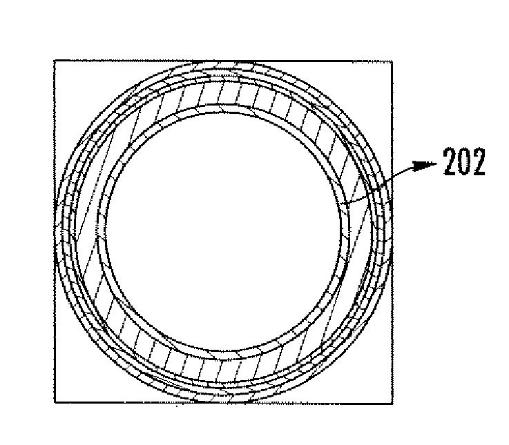
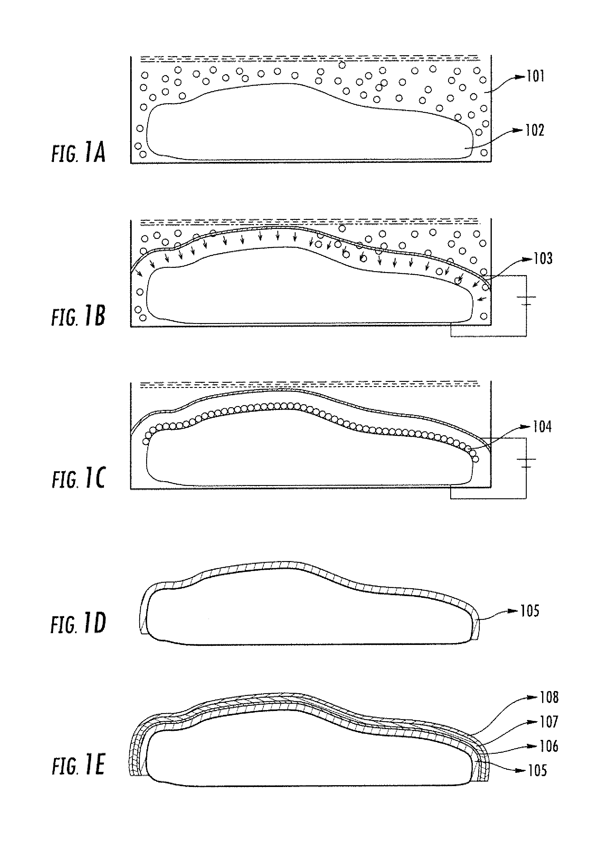
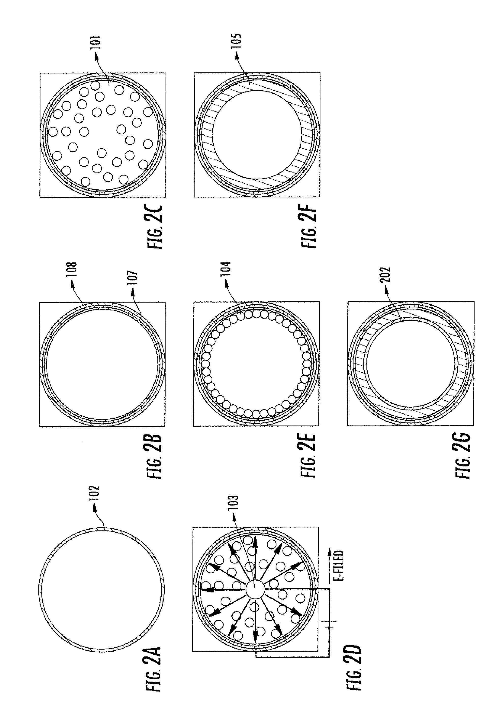
[0018]FIGS. 1A to 1E and 2A to 2G illustrate examples for forming CIGS / CZTS layers on complexly shaped surfaces of fabricated objects, which may be greatly different in size and geometry. Corresponding features, appearing in both FIGS. 1 and 2, are designated by the same number. FIGS. 1A to 1E illustrate one implementation of the present invention in which a CIGS / CZTS solar cell is deposited on a car bo...


PUM

PropertyMeasurementUnit
Temperatureaaaaaaaaaa
Thicknessaaaaaaaaaa
Thicknessaaaaaaaaaa

Abstract

Methods for fabricating a photovoltaic device on complexly shaped fabricated objects, such as car bodies are disclosed. Preferably the photovoltaic device includes absorber layers comprising Copper, Indium, Gallium, Selenide (CIGS) or Copper, Zinc, Tin, Sulfide (CZTS). The method includes the following steps: a colloidal suspension of metal surface-charged nanoparticles is formed; electrophoretic deposition is used to deposit the nanopartieles in a metal thin film onto a complexly shaped surface of the substrate; the metal thin film is heated in the presence of a chalcogen source to convert the metal thin film into a metal chalcogenide thin film layer; a buffer layer is formed on the metal chalcogenide thin film layer using a chemical bath deposition; an intrinsic zinc oxide insulating layer is formed adjacent to a side of the buffer layer, opposite the metal chalcogenide thin film layer, by chemical vapor deposition; and finally, a transparent conducting oxide is formed adjacent to a side of the intrinsic zinc oxide, opposite the buffer layer, by chemical vapor deposition.

Description

RELATED APPLICATIONS[0001]The present application claims the benefit of U.S. application Ser. No. 12 / 910,929, filed on Oct. 25, 2010 as a continuation-in-part application of that application. U.S. application Ser. No. 12 / 910,929, filed on Oct. 25, 2010, is hereby incorporated by reference in its entirety.STATEMENT REGARDING FEDERALLY SPONSORED RESEARCH[0002]NONE.TECHNICAL FIELD[0003]The present invention relates to fabrication of a photovoltaic absorber layer and a photovoltaic device incorporating the layer wherein the photovoltaic absorber layer is fabricated by electrophoretic deposition of nanoparticles of an absorptive material on complexly shaped surfaces of fabricated objects.BACKGROUND[0004]Compound semiconductors based on an absorber layer of chalcopyrite or kesterite are some of the most promising materials for solar cells. The chalcopyrite material Cu(In,Ga)Se2 (CIGS), is a direct bandgap semiconductor that has demonstrated solar-to-electrical energy conversion efficienci...

Claims


Application Information

Patent Timeline
IPC IPC(8): H01L31/0352
CPCC25D5/48C25D15/02H01L31/0322Y02E10/541H01L31/03923H01L31/0747H01L31/035281
Inventor HAGEDORN, KEVIN V.GUO, WEILIU, BING
Owner IMRA AMERICA
Why Eureka
Try Eureka