Systems and methods for fabricating self-aligned memory cell

a self-aligning and memory cell technology, applied in the direction of basic electric elements, electrical equipment, semiconductor devices, etc., can solve the problems of volatile drams and power requirements, and achieve the effects of low cost, high density storage, and low cos

Active Publication Date: 2012-05-17
4D S
View PDF2 Cites 50 Cited by
  • Summary
  • Abstract
  • Description
  • Claims
  • Application Information

AI Technical Summary

Benefits of technology

[0013]Advantages of the invention may include one or more of the following. The system provides a low-cost high density solid state memory device. The memory units can be interconnected within a wafer, and the wafers are interconnected in a stacked wafer construction of a memory system. The resulting semiconductor device offers high density storage at a very low cost. Moreover, the process can be done at low temperature. The substrate temperature in forming a thin film approximately at the range of 300-400 deg. C. and the process requires a short time. Since the thin film is formed at a very low temperature during substantially the whole process, the process can be applied to a highly integrated device to deposit an additional memory layer with a plurality of elements without damaging other elements previously deposited using conventional deposition.

Problems solved by technology

DRAMs are volatile and thus require power to maintain the data from being lost.

Method used


Image

  • Systems and methods for fabricating self-aligned memory cell
  • Systems and methods for fabricating self-aligned memory cell
  • Systems and methods for fabricating self-aligned memory cell

Examples


Embodiment Construction

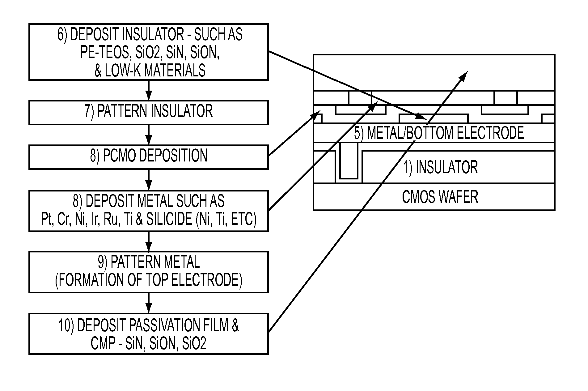
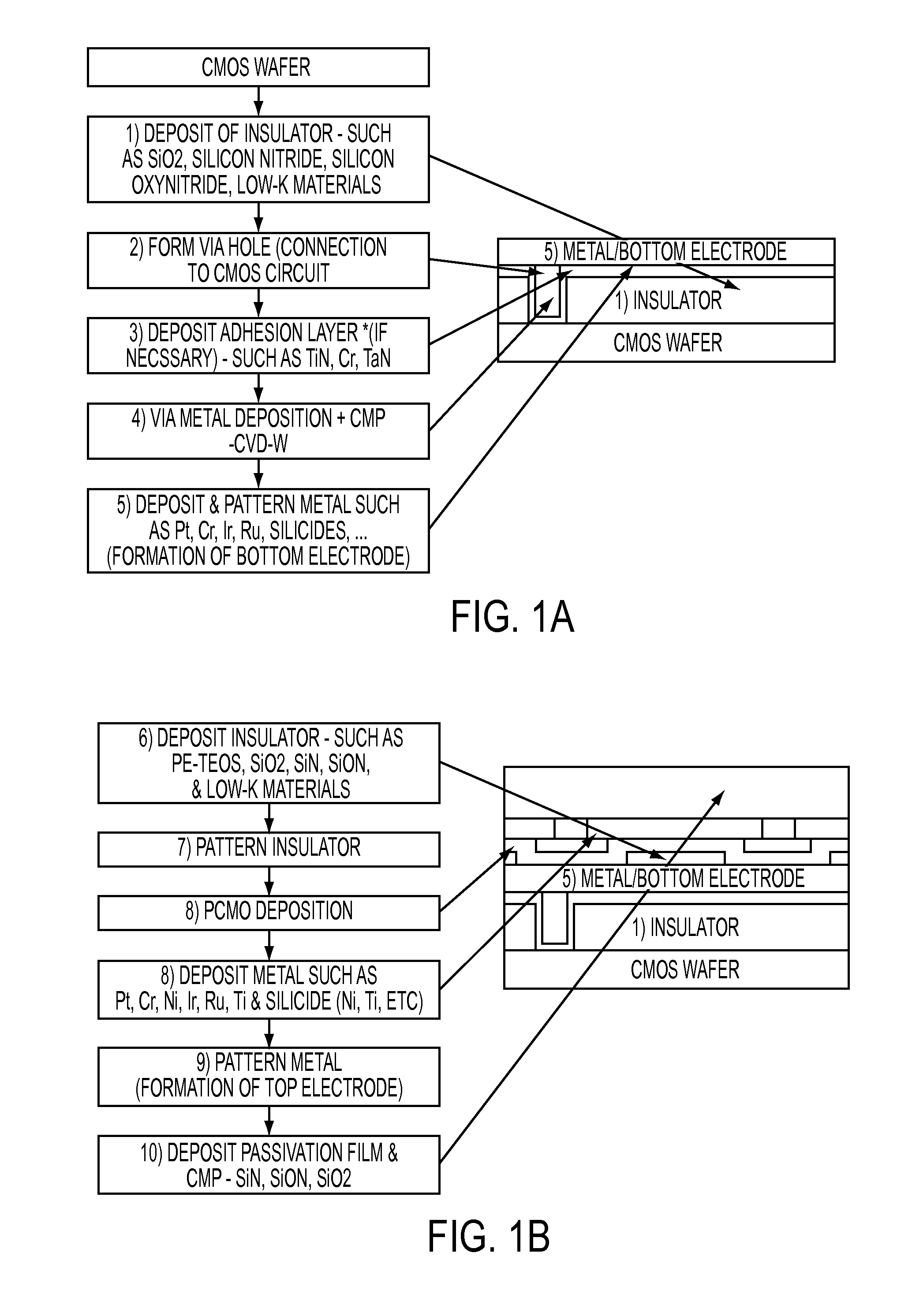
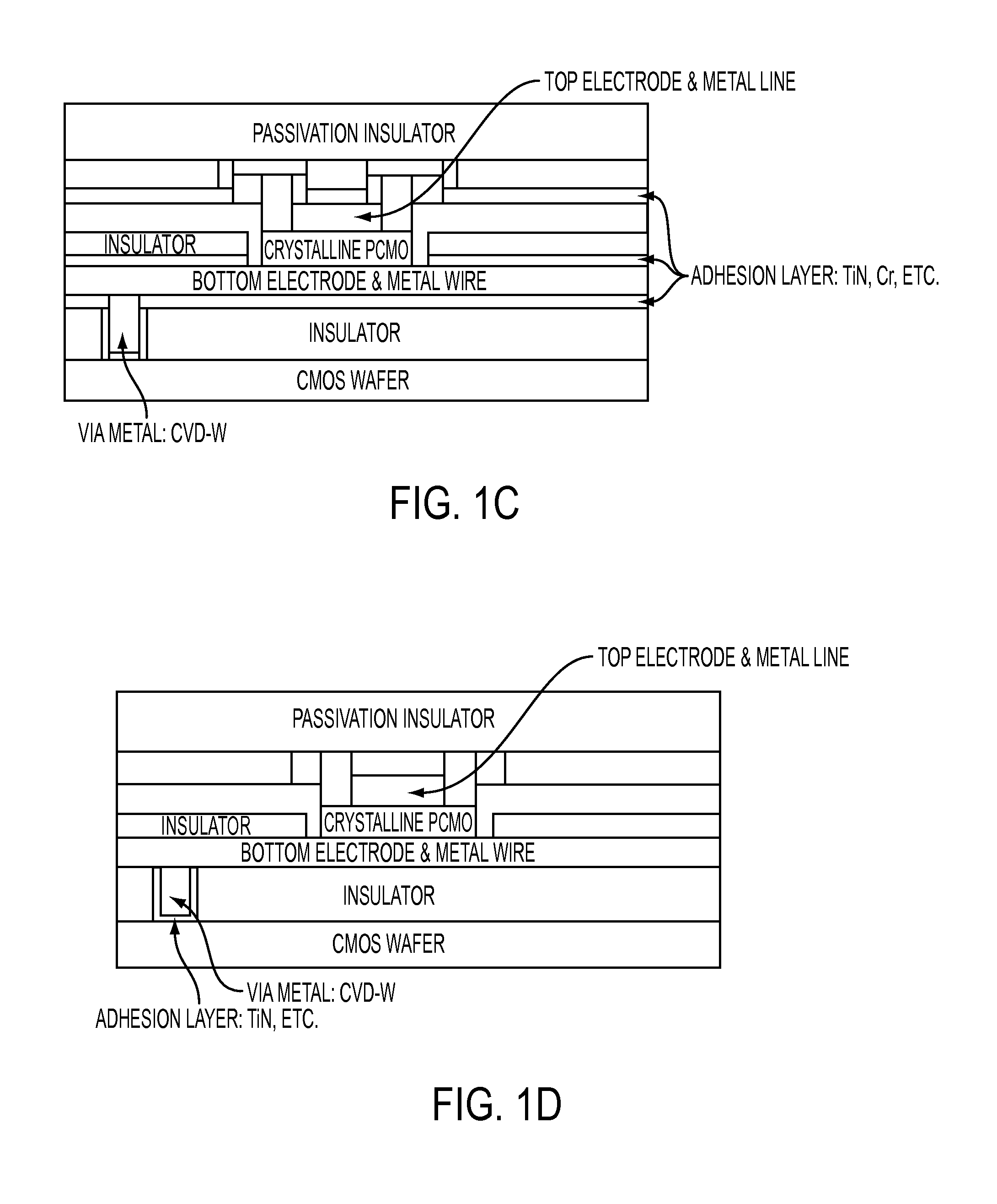
[0024]Referring now to the drawings in greater detail, there is illustrated therein structure diagrams for a semiconductor processing system and logic flow diagrams for processes a system will utilize to deposit a memory device, as will be more readily understood from a study of the diagrams.

[0025]FIGS. 1A-1B show an exemplary process to fabricate a self-aligned memory cell. The process uses CMOS wafers and conventional CMOS circuits or structures may be formed on the wafer prior to the memory cell fabrication. One or more electronic devices can be formed on the wafer. The process forms non-volatile memory such as RRAM. Unlike conventional DRAM, which uses electrical cells (e.g., capacitors) to store data, RRAM uses resistance cells. Because resistance memory cells maintain their state even when power is removed, RRAM possesses a distinct advantage over electrical cells.

[0026]Turning now to FIG. 1A, the process deposits an insulator such as silicon dioxide, silicon nitride, silicon ...


PUM

PropertyMeasurementUnit
junction resistanceaaaaaaaaaa
resistanceaaaaaaaaaa

Abstract

Systems and methods are disclosed to form a resistive random access memory (RRAM) by forming a first metal electrode layer; depositing an insulator above the metal electrode layer and etching the insulator to expose one or more metal portions; depositing a Pr1-XCaXMnO3 (PCMO) layer above the insulator and the metal portions, wherein X is between approximately 0.3 and approximately 0.5, to form one or more self-aligned RRAM cells above the first metal electrode; and depositing a second metal electrode layer above the PCMO layer.

Description

CROSS-REFERENCE TO RELATED APPLICATIONS[0001]Under 35 USC §120, this application is a divisional application and claims the benefit of priority to U.S. patent application Ser. No. 11 / 486,472, filed Jul. 14, 2006, entitled “SYSTEMS AND METHODS FOR FABRICATING SELF-ALIGNED MEMORY CELL”, and is related to U.S. patent application Ser. No. 11 / 388,528, filed Mar. 25, 2006, entitled “SYSTEMS AND METHODS FOR FABRICATING SELF-ALIGNED MEMORY CELL”, all of which is incorporated herein by reference.FIELD OF THE INVENTION[0002]The present invention relates generally to a self-aligned storage' node for a memory device such as a nonvolatile memory device.BACKGROUND OF THE INVENTION[0003]A memory device such as random access memory (RAM) is a semiconductor device for storing digital information. Data, as digital information, can be written to and read from a RAM. RAMs are fabricated using integrated circuit technology. For example, a DRAM is made of many storage nodes or memory cells and each memor...

Claims


Application Information

Patent Timeline
Patent Type & Authority Applications(United States)
IPC IPC(8): H01L45/00
CPCH01L45/16H01L45/14H01L27/2481H01L45/1233H01L45/147H01L45/04H10B63/84H10N70/20H10N70/8836H10N70/011H10N70/826H10N70/881
Inventor NAGASHIMA, MAKOTO
Owner 4D S
Why Eureka
Try Eureka