Method for manufacturing semiconductor device

a semiconductor and manufacturing method technology, applied in the direction of semiconductor devices, basic electric elements, electrical appliances, etc., can solve the problems of oxygen deficiency, etc., and achieve the effect of reducing leakage current between a source and a drain and preventing deformation

Inactive Publication Date: 2012-07-12
SEMICON ENERGY LAB CO LTD
View PDF20 Cites 40 Cited by
  • Summary
  • Abstract
  • Description
  • Claims
  • Application Information

AI Technical Summary

Benefits of technology

[0007]When side surfaces of an oxide semiconductor layer are processed into a desired shape in order to manufacture a semiconductor device to which an oxide semiconductor is applied, the side surfaces of the oxide semiconductor layer are exposed to a vacuum (a reduced-pressure atmosphere or a reducing atmosphere) in a reaction chamber while they are in an active state. Therefore, oxygen is extracted from the side surfaces of the oxide semiconductor layer to the reaction chamber and defects (oxygen deficiency) are caused. Such defects (oxygen deficiency) reduce the resistance of a region in which the defects (oxygen deficiency) exist as donors, which causes leakage current between a source and a drain.
[0008]An object of one embodiment of the present invention is to provide a method for manufacturing a semiconductor device by which the semiconductor device can be manufactured while oxygen sufficiently exists on side surfaces of an oxide semiconductor layer.
[0009]Another object of one embodiment of the present invention is to provide a semiconductor device in which the amount of defects (oxygen deficiency) in an oxide semiconductor layer are sufficiently small and leakage current between a source and a drain is suppressed.
[0010]One embodiment of the present invention is a method for manufacturing a semiconductor device including the following steps: after first heat treatment is performed on an oxide semiconductor film, the oxide semiconductor film is processed to form an oxide semiconductor layer; immediately after that, side walls of the oxide semiconductor layer are covered with an insulating oxide; and in second heat treatment, the side surfaces of the oxide semiconductor layer are prevented from being exposed to a vacuum and defects (oxygen deficiency) in the oxide semiconductor layer can be reduced. An insulating layer provided so as to cover the side walls of the oxide semiconductor layer is a sidewall insulating layer. A sidewall insulating film is formed entirely and processed, whereby the sidewall insulating layer is formed. It is preferable that heat treatment be further performed between after the sidewall insulating film is formed and before the sidewall insulating layer is formed.
[0014]According to one embodiment of the present invention, defects (oxygen deficiency) in an oxide semiconductor layer of a semiconductor device can be sufficiently reduced and leakage current between a source and a drain can be made low.

Problems solved by technology

Therefore, oxygen is extracted from the side surfaces of the oxide semiconductor layer to the reaction chamber and defects (oxygen deficiency) are caused.
Such defects (oxygen deficiency) reduce the resistance of a region in which the defects (oxygen deficiency) exist as donors, which causes leakage current between a source and a drain.

Method used


Image

  • Method for manufacturing semiconductor device
  • Method for manufacturing semiconductor device
  • Method for manufacturing semiconductor device

Examples


embodiment 1

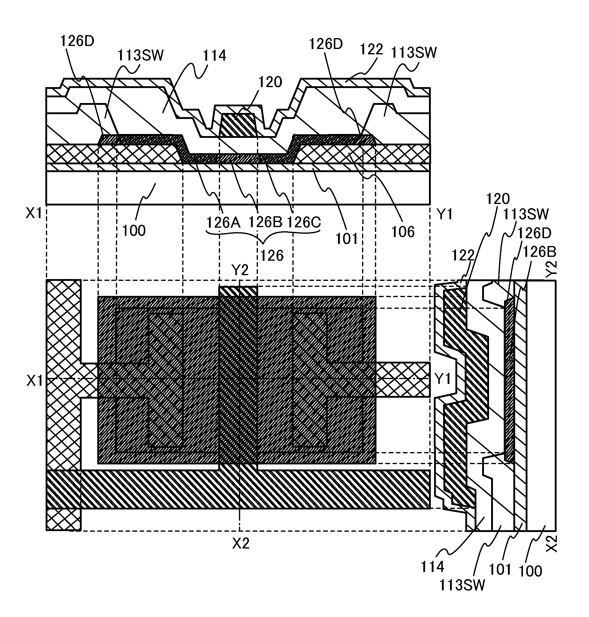
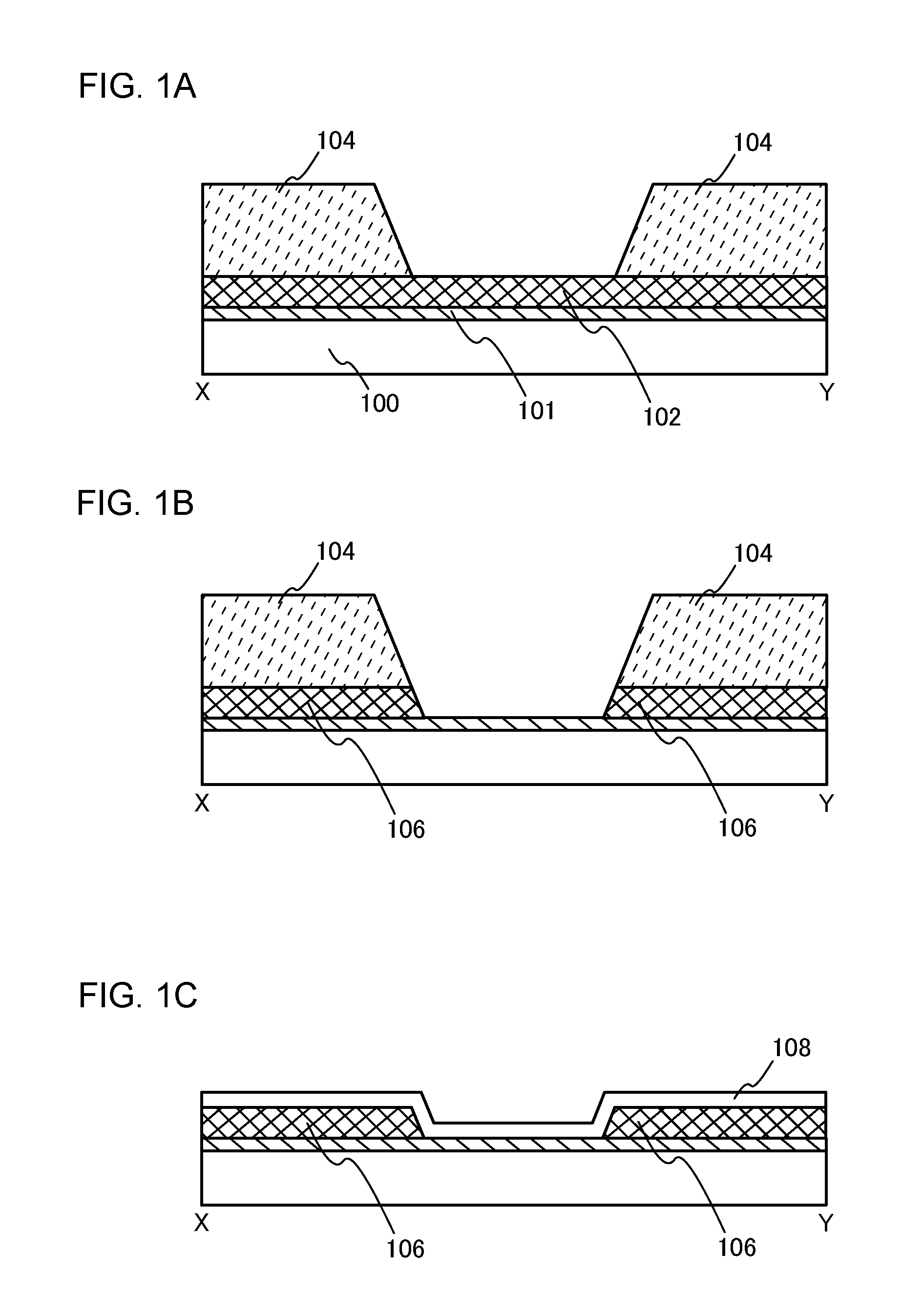
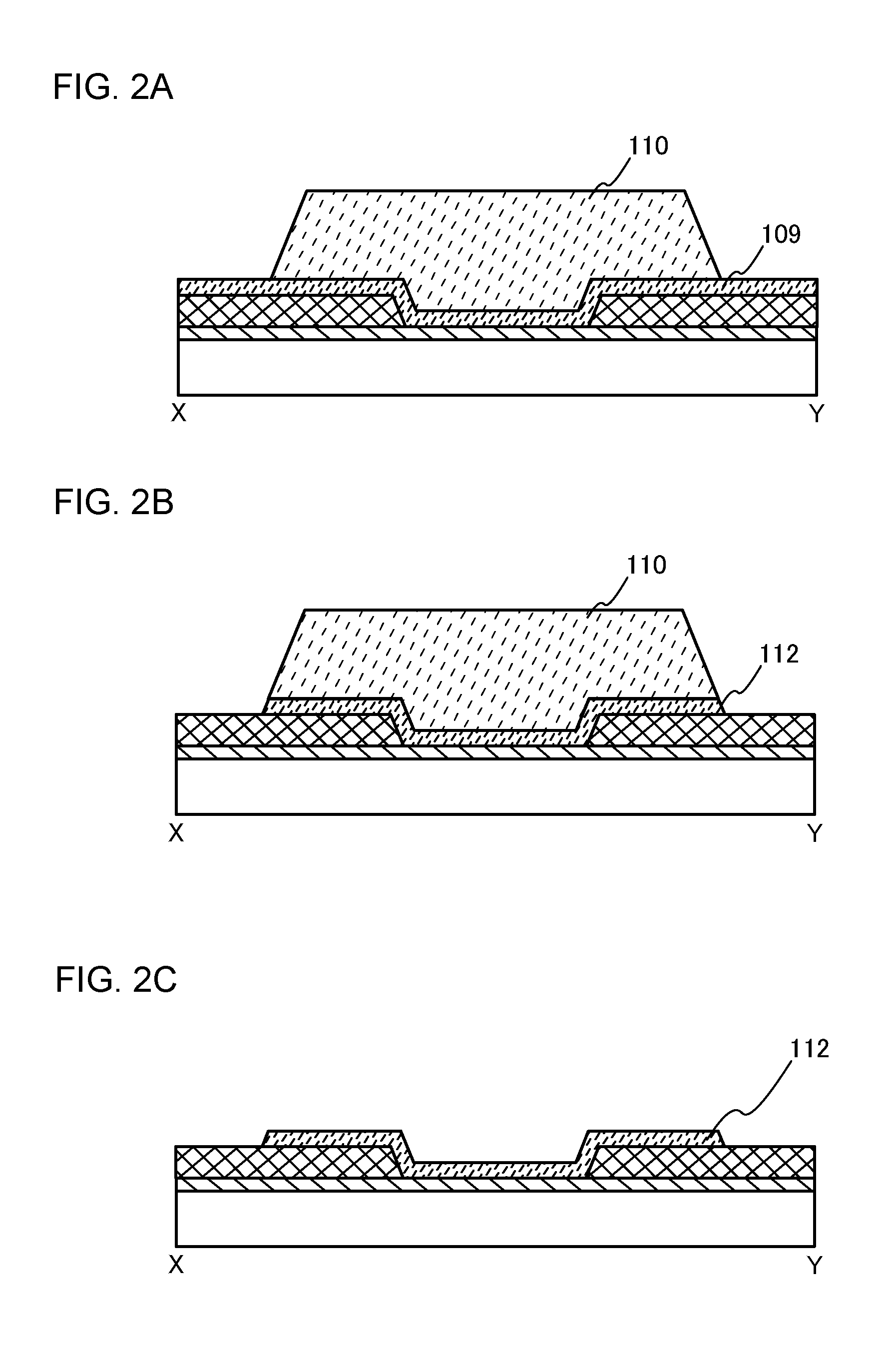
[0038]In this embodiment, a method for manufacturing a semiconductor device which is one embodiment of the present invention is described. Specifically, a method for manufacturing a transistor is described.

[0039]A method for manufacturing a transistor of this embodiment is as follows: a base insulating layer 101 and a first conductive film 102 are formed over a substrate 100; a first etching mask 104 is formed over the first conductive film 102; a first conductive layer 106 is formed by processing the first conductive film 102 using the first etching mask 104; the first etching mask 104 is removed; a first oxide semiconductor film 108 is formed over the first conductive layer 106; a second oxide semiconductor film 109 is processed by performing at least first heat treatment on the substrate 100; a second etching mask 110 is formed over the second oxide semiconductor film 109; a first oxide semiconductor layer 112 is formed by processing the second oxide semiconductor film 109 using ...

embodiment 2

[0161]In this embodiment, an application example of the transistor described in Embodiment 1 will be described.

[0162]FIG. 7A illustrates an example of a circuit diagram of a memory element (hereinafter, denoted by a memory cell) included in a semiconductor device. The memory cell illustrated in FIG. 7A includes a transistor 200 in which a channel formation region is formed using a material other than an oxide semiconductor (e.g., silicon, germanium, silicon carbide, gallium arsenide, gallium nitride, an organic compound, or the like) and a transistor 202 in which a channel formation region is formed using an oxide semiconductor.

[0163]The transistor 202 in which the channel formation region is formed using an oxide semiconductor is manufactured by the method for manufacturing a semiconductor device of one embodiment of the present invention which is described in Embodiment 1.

[0164]As illustrated in FIG. 7A, a gate of the transistor 200 is electrically connected to one of a source and...

embodiment 3

[0192]In this embodiment, an application example of the transistor described in Embodiment 1, which is different from the example described in Embodiment 2, will be described.

[0193]In this embodiment, a memory cell including a capacitor and a semiconductor memory device will be described. A memory cell 300 illustrated in FIG. 9A includes a first wiring SL, a second wiring BL, a third wiring S1, a fourth wiring S2, a fifth wiring WL, a transistor 302 (a first transistor), a transistor 304 (a second transistor), and a capacitor 306. In the transistor 302, a channel formation region is formed using a material other than an oxide semiconductor, and in the transistor 304, a channel formation region is formed using an oxide semiconductor.

[0194]The transistor 304 in which the channel formation region is formed using an oxide semiconductor is manufactured by the method for manufacturing a semiconductor device of one embodiment of the present invention which is described in Embodiment 1.

[019...


PUM


Abstract

To provide a semiconductor device in which desorption of oxygen from side surfaces of an oxide semiconductor layer is prevented, defects (oxygen deficiency) in the oxide semiconductor layer are sufficiently reduced, and leakage current between a source and a drain is suppressed. The semiconductor device is manufactured through the following steps: after first heat treatment is performed on an oxide semiconductor film, the oxide semiconductor film is processed to form an oxide semiconductor layer; immediately after that, side walls of the oxide semiconductor layer are covered with an insulating oxide; and in second heat treatment, the side surfaces of the oxide semiconductor layer are prevented from being exposed to a vacuum and defects (oxygen deficiency) in the oxide semiconductor layer are reduced. Side walls of the oxide semiconductor layer are covered with sidewall insulating layers. The semiconductor device has a TGBC structure.

Description

BACKGROUND OF THE INVENTION[0001]1. Field of the Invention[0002]The present invention relates to a semiconductor device and a manufacturing method thereof. Note that in this specification, a semiconductor device refers to a semiconductor element itself or a device including a semiconductor element. As an example of such a semiconductor element, a transistor (a thin film transistor and the like) can be given. In addition, a semiconductor device also refers to a display device such as a liquid crystal display device.[0003]2. Description of the Related Art[0004]Semiconductor devices have been indispensable to our life. Silicon has been mainly used as conventional semiconductor materials applied to semiconductor devices. However, in recent years, as semiconductors applied to semiconductor devices, oxide semiconductors have attracted attention. Semiconductor devices in which a Zn—O-based metal oxide or an In—Ga—Zn—O-based metal oxide is used as oxide semiconductors are disclosed in Paten...

Claims


Application Information

Patent Timeline
Patent Type & Authority Applications(United States)
IPC IPC(8): H01L21/336
CPCH01L29/7869H01L29/66742H01L29/78618
Inventor YAMAZAKI, SHUNPEI
Owner SEMICON ENERGY LAB CO LTD
Why Eureka
Try Eureka