Structured silicon battery anodes
a battery anode and silicon technology, applied in the field of structured silicon battery anodes, can solve the problems of increasing the stress in the crystal structure, the practicable limit is 300-330 mah/g, and the silicon has serious expansion/contraction problems during cycling, so as to improve the cycling behavior, improve the cycling effect, and improve the effect of cycling
- Summary
- Abstract
- Description
- Claims
- Application Information
AI Technical Summary
Benefits of technology
Problems solved by technology
Method used
Image
Examples
example 1
[0049]For all experiments, prime grade, boron doped, p-type and single-side polished silicon wafers from Siltronix™ and University™ wafer were used. All the wafers were 275±25 microns thick and had resistivities between 14-22 Ωcm and 10-30 Ωcm with face orientation of (100).
[0050]Porous silicon (pSi) was generated by etching crystalline silicon in aqueous hydrofluoric acid (HF) electrolytes in a standard electrochemical cell made out of Teflon.™ A Viton™ O-ring was used to seal the cell. The wafers were pressed against the gasket with an aluminum plate. Wire form platinum was immersed in the solution as the counter electrode. All etching was performed under constant current conditions, with proper current provided by an Agilent™ E3612A DC Power Supply. The unpolished side of the wafer was coated with aluminum to reduce the contact resistance to the aluminum back plate.
[0051]For all the results reported here, the etchings are performed using dimethylformamide (DMF) and a 49% HF solut...
example 2
[0065]The porosity, thickness, pore diameter and microstructure of porous silicon (pSi) depends on the anodization conditions. For a fixed current density, the porosity decreases as HF concentration increases. Additionally, the average depth increases and porosity decreases with increasing HF concentration (Table 2). Fixing the HF concentration and current density, the porosity increases with the thickness (Table 3). Increasing current density increases the pore depth and porosity (Table 4). This happens because of the extra chemical dissolution of the porous silicon layer in HF. The thickness of a porous silicon layer is determined by the time that the current density is applied, that is, the anodization times. Another advantage of the formation process of porous silicon is that once a porous layer has been formed, no more electrochemical etching occurs for it during the following current density variations.27
TABLE 2Effect of etch time on pSi structure.ConcentrationPorosityCurrent...
example 3
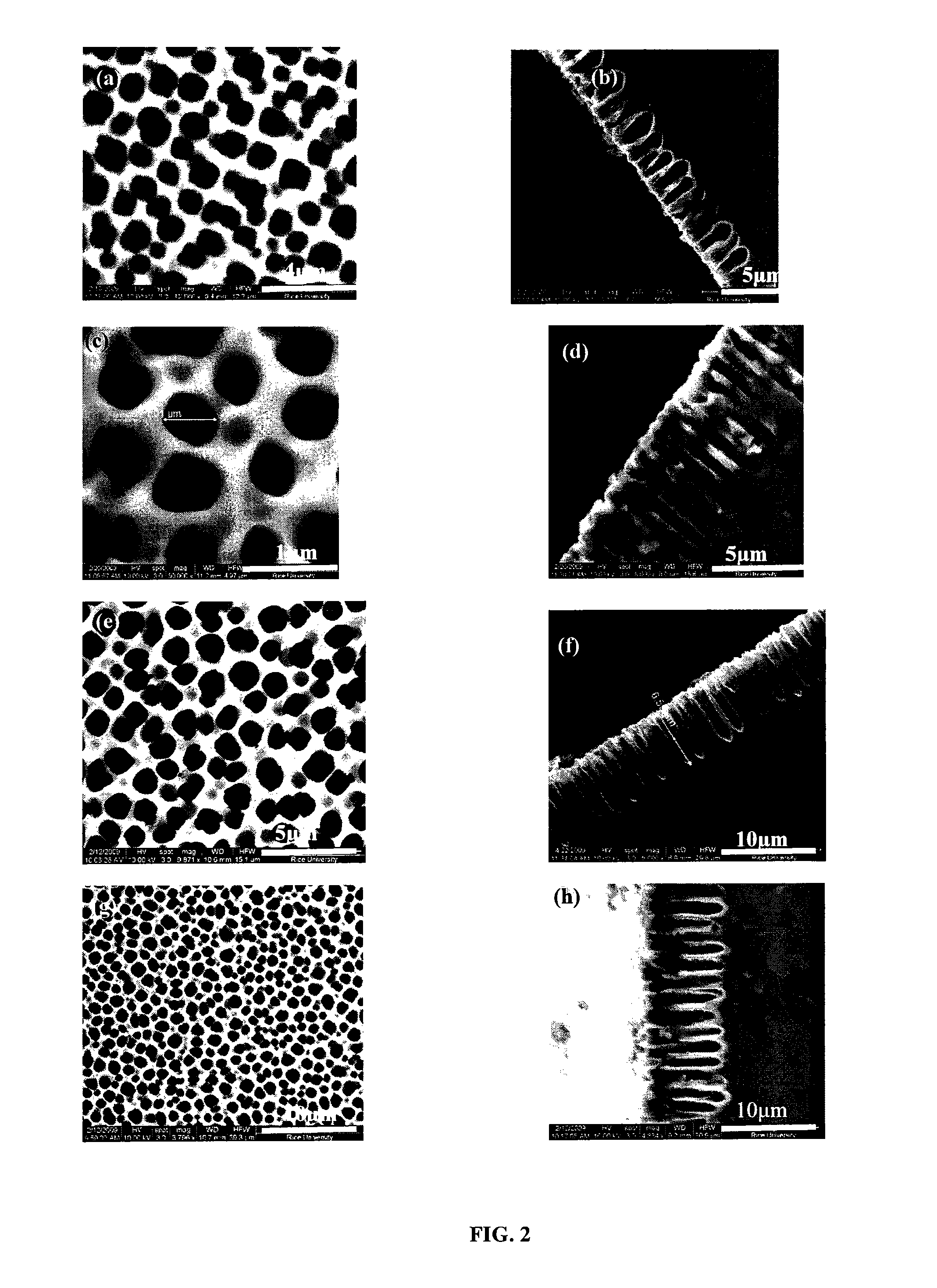
[0066]The cycle life and specific capacity of pSi structures with different porosities but the same average pore depth were compared. Etching parameters for creating same depth and different porosity of porous silicon (pSi) are given in (Table 5). Shown in the FIG. 8 are top and cross-sectional views of pSi samples, with the same depth and differing porosity.
TABLE 5Etching parameter for creating same average depth and different porosity.TimeAveragePorositySampleFIGS.CurrentConcentration(min)Depth(%)E8a 8b8 mAHF:DMF,1805.660 ± 2%1:35 mlF8c 8d5 mAHF:DMF, 1805.4936 ± 2%0.7:30 ml
[0067]FIG. 9 shows the specific capacities versus cycles for sample E and sample F of different porosity and same average depth. The cell is charge and discharged between 0.09 to 1.5 V, at a rate of 200 μA. The average pore depth of sample is 5.6 and 5.49 μm. The mass of the pSi calculated form Eq. 3 was 0.00098 g. It is seen that specific capacity as well as cycle life for the sample F were better as compared t...
PUM
| Property | Measurement | Unit |
|---|---|---|
| pore depth | aaaaa | aaaaa |
| diameter | aaaaa | aaaaa |
| charge capacity | aaaaa | aaaaa |
Abstract
Description
Claims
Application Information


