Compound semiconductor light-receiving element array

a light-receiving element and semiconductor technology, applied in the field of compound semiconductor photodiode arrays, can solve the problems of high cross-talk between the elements, invalid light shielding masks, and problems in production yield, and achieve the effects of stable over time, easy manufacturing, and uniform characteristics

Active Publication Date: 2012-11-15
IRSPEC CORP
View PDF3 Cites 9 Cited by
  • Summary
  • Abstract
  • Description
  • Claims
  • Application Information

AI Technical Summary

Benefits of technology

[0024]In the structure of the present invention, the photosensitive layer is completely isolated from adjacent elements by a potential barrier in the horizontal direction built in the PN junction so that it is possible to prevent photo-generated carriers to flow into adjacent elements. Also, since the photosensitive layer is separated from the surface layer by the window layer, it is not affected by the quality of the dielectric surface passivation film and stable over time. In addition, since the crosstalk can be suppressed without forming the mesa structure or providing a light shielding mask between the elements, it becomes easier to manufacture an array of narrow pitch. Since the PN junction to form the photo-detection region is made by epitaxial growth rather than by thermal diffusion method, the characteristics are uniform and production yield is high. This point is important from the viewpoint of productivity particularly in fabricating large scale arrays.
[0025]The epitaxial growth allows to control the layer thickness in a few nanometers scale and by making the window layer formed by epitaxial growth less than 0.2 μm in thickness, so that the PN junction depth can be formed thinner than that is formed by thermal diffusion method. The detectable short wavelength edge of the conventional InP / InGaAs PD with the InP window layer was about 900 nm but according to the present invention, the short wavelength side can be extended to about 500 nm.
[0026]In addition, for the PD according to the present invention, it is possible to form electrodes for the first and second conductivity types only on the surface side, therefore, the substrate and the buffer layer needed for epitaxial growth do not have to be used as a current path. In this case, even if the crystal defects existing in the interface between the substrate and the buffer layer or defects due to lattice mismatch in the buffer layer, it is possible to avoid the influence of dark current due to such defects. Therefore, the photo-detection wavelength range of the photo absorbing layer can be greatly extended by using a mixed crystal semiconductor of which lattice constant is much different from that of substrate.
[0027]In addition, by increasing the potential barrier only for minority carriers in the surface window layer selectively, light generated carriers can lead to electrodes without retention. Because common electrodes of conventional planar PDs are N type and electrodes of separated array elements are P type, it is necessary to bias the common electrode to the positive potential. Therefore, it is necessary to insulate the substrate of the PD from the package.
[0028]On the other hand, in the present invention, the signal output electrodes, that is, positive potential can be formed on the N-type layer of each PD element and the common electrode can be made on the P type layer. Therefore, the virtual ground voltage of an ROIC is set to about ½ of the bias voltage usually, so that the appropriate bias voltage can be obtained by setting the common electrode at zero potential and just connecting each array element to the input current terminal of the ROIC.

Problems solved by technology

This kind of structures are simple in fabrication process but have disadvantage that the cross-talk between the elements is high.
This method is effective to prevent the photo-excited current in the gap between the elements but it cannot prevent carriers generated just under the element from flowing into adjacent elements completely and moreover, the light shielding mask is invalid when arrays are configured to receive incident light from the substrate side.
And also, to form a light-shielding mask on arrays with a narrow pitch less than 10 few micrometers induces problems in the production yield.
However, the metallurgical PN junction is exposed to the surface in the mesa structure formed in a compound semiconductor so that a surface leak current is significantly increased.
The large surface leak current causes a noise and deteriorates the minimum light receiving sensitivity.
Such accumulated electrons induce unstable electrical phenomenon as to invert the I type mesa surface area and deteriorate PD characteristics with time.
In these structures, the front of the impurity diffused layer requires to be kept inside in a buffer layer with the large energy band gap, and the fabrication process was complicated as acceptable control range of process conditions is narrow.
In addition, in the case of the document 7, in order to form a PN junction of the photosensitive layer by impurity diffusion, there is a problem that the junction is formed in a relatively deep position, which reduces the sensitivity in the short wavelength side.

Method used


Image

  • Compound semiconductor light-receiving element array
  • Compound semiconductor light-receiving element array
  • Compound semiconductor light-receiving element array

Examples


example 1

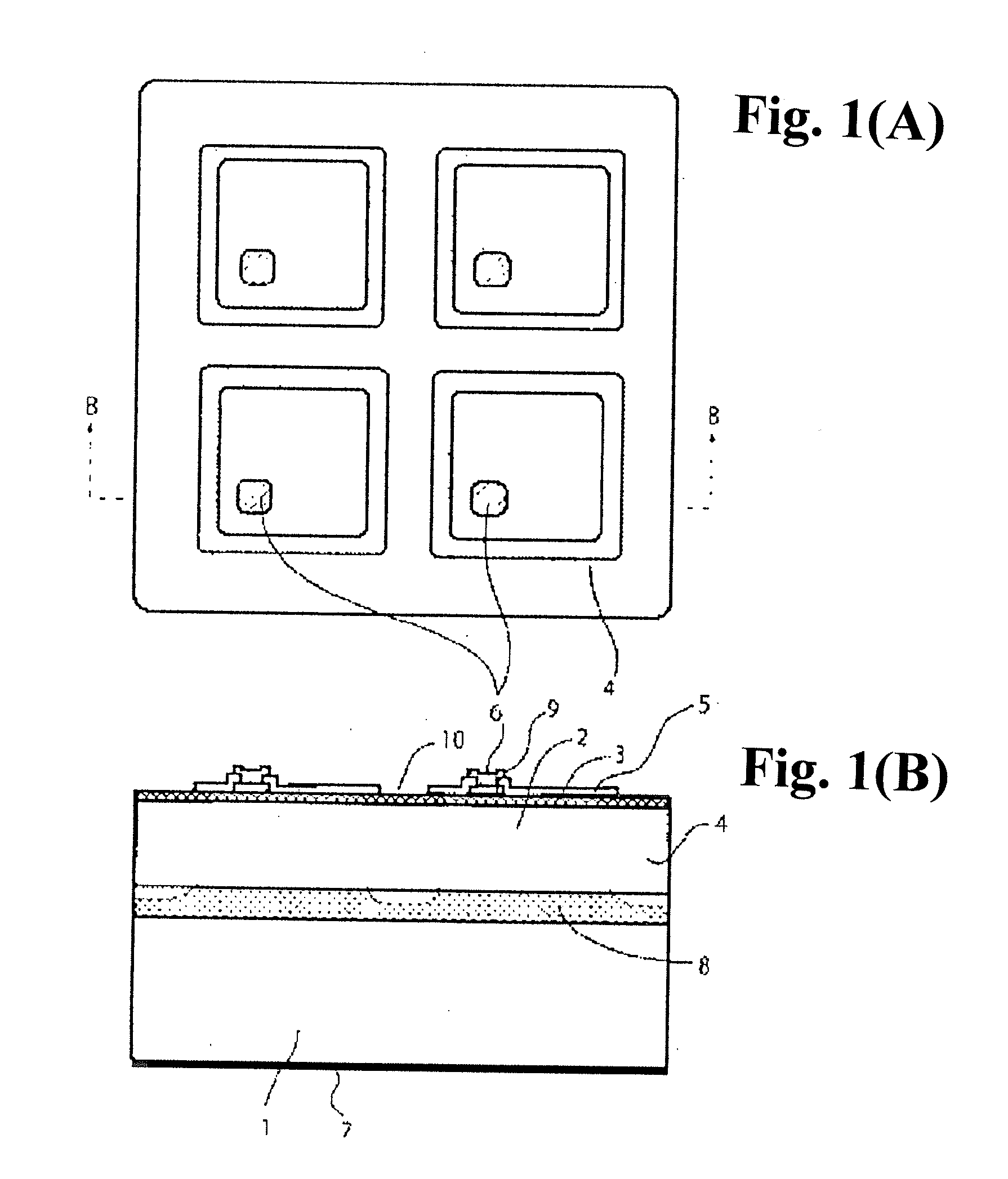
[0042]FIGS. 1(A) and 1(B) show an example of a planar array PD as an embodiment of this invention which is formed by deep zinc diffusion. FIG. 1(A) is a plan view, FIG. 1(B) shows a cross-sectional view of the element along B-B line. The carrier concentration of a P-type InP substrate is set to the order of 1018 to 1019 cm−3 which enables to obtain ohmic characteristics easily when the P side electrode 7 is formed on the substrate. An InGaAs photosensitive layer 2 can be an undoped I (intrinsic) layer or a low concentration N-type layer with 1014 to 1015 cm−3 carrier concentration. The InGaAs photosensitive layer 2 is used as a light-absorbing layer and can be replaced with any composition of InxGa1-xAsyP1-y in order to provide the selectivity of the detection wavelength, or it is also possible to change to an InAlAs system composition to extend the detection wavelength. The thickness of the photosensitive layer 2 is determined by the conditions to optimize the response speed and qu...

example 2

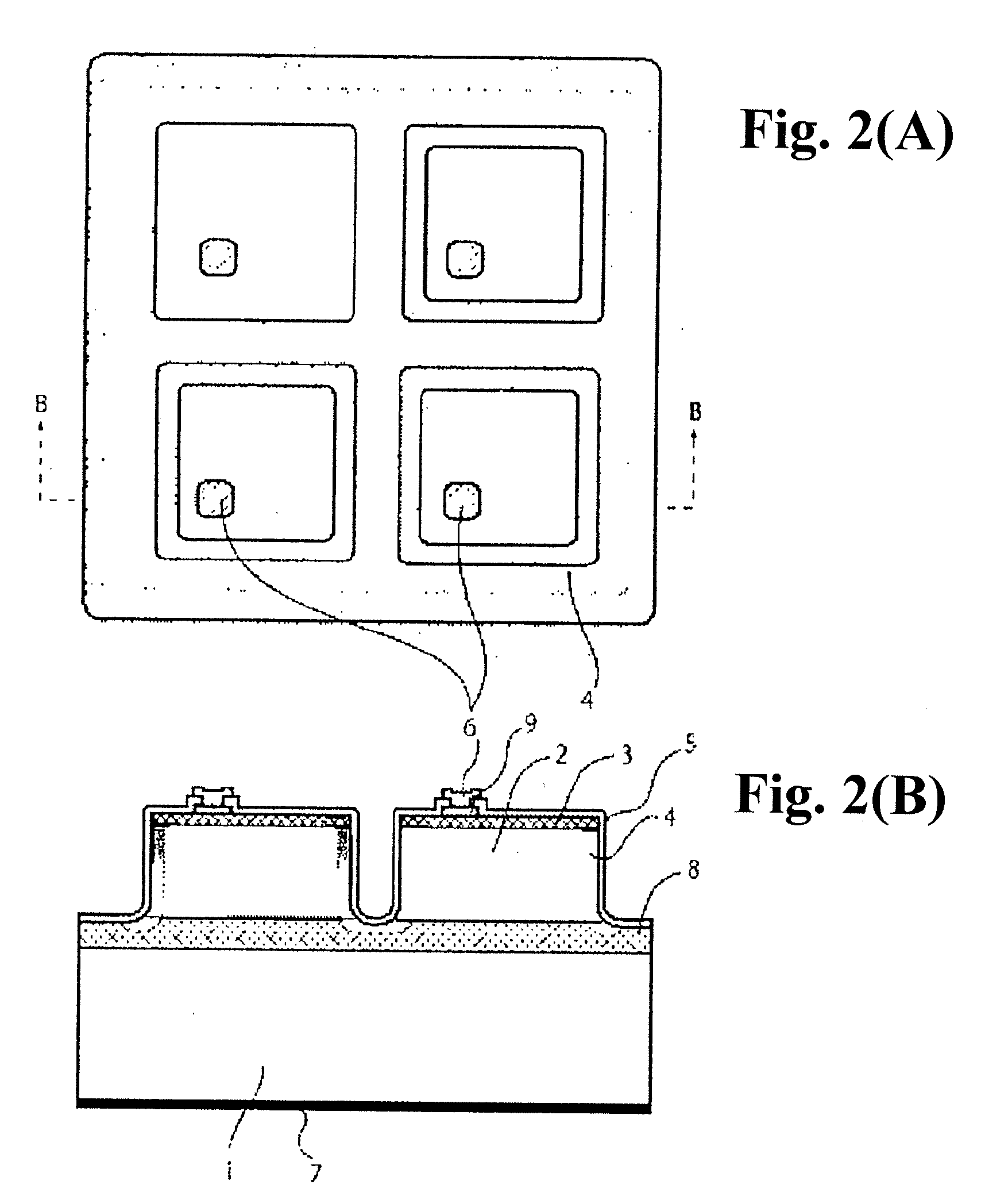
[0045]FIG. 2(A) shows a plan view and 2(B) shows cross-sectional view of a mesa isolated PD to the direction of the arrow B as an embodiment of the present invention. An island shape was formed by mesa etching of a wafer formed of an InGaAs photosensitive layer 2 and an N-type InP window layer 3, which were stacked on a P-type InP substrate 1. Then, a P-type layer 4 was formed by diffusing zinc selectively only to the mesa side and bottom. An N-type InGaAs contact layer was left in an island shape on the part of N-type InP window layer 3. The top surface, the mesa side and bottom were covered with a dielectric layer 5 formed of a silicon nitride film. Finally, an N-side electrode 6 was formed on the opening of the silicon nitride film. A P-type InP barrier layer is a buffer layer formed between a substrate and laminated epitaxial layers in order to improve the quality of the epitaxial crystal layer, and simultaneously works as an etch stop layer using etch selectivity during the mes...

example 3

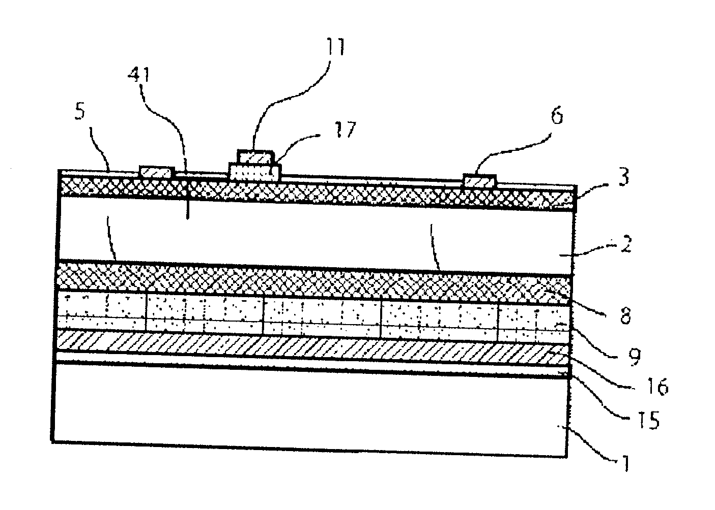
[0050]FIG. 3 shows a one-dimensional array and two-dimensional array, in which incident light is illuminated on their substrate sides. In these cases, the P-type electrodes 11 are formed in contact with the diffused surface 4, and they are bonded with a read-out integrated circuit (ROIC) or a circuit board 12 via metal bumps 13. Such a flat surface structure array as shown in FIG. 1 is advantageous in terms of yield and reliability, because of easiness in the device fabrication process compared with mesa type arrays.


PUM


Abstract

An array structure solves issues that exist in conventional compound semiconductor photodiode arrays, such as large cross talk, large surface leaks, large stray capacitance, narrow detection wavelength bands, and bad manufacturing yield, simultaneously. A photodiode array has, laminated upon a semiconductor substrate, a buffer layer (8) with a broad forbidden band width, an I-type (low concentration photosensitive layer (2) with a narrow forbidden band width, and an n-type semiconductor window layer (3) with a broad forbidden band width, wherein photodiode elements are electrically separated from adjacent elements, by doping the periphery of the p-type impurity, and the detection wavelength band is expanded, by making the n-type window layer (3) on the photosensitive layer (2) a thinner layer with crystal growth.

Description

TECHNICAL FIELD [0001]This invention relates to a compound semiconductor photodiode array having low dark current, wider wavelength range and very little crosstalk between the elements.BACKGROUND ART [0002]Photodetectors comprised of a compound semiconductor material system have sensitivity in the wavelength regions that silicon detectors do not cover have been widely used particularly in the infrared region as the most sensitive photodetector. Compound semiconductor photodiode arrays are in broad demand such as sensors for infrared spectroscopy, monitors for optical communications with wavelength division multiplexing, infrared image sensors and various industrial measurements. Compound semiconductor arrays mostly used in many ways are photodiode arrays having the light receiving layer of the InGaAs layer formed by epitaxial growth on the InP substrate. For the detection of longer wavelength of the near-mid infrared region, photodiode arrays comprised of the InSb system, the InAs s...

Claims


Application Information

Patent Timeline
Patent Type & Authority Applications(United States)
IPC IPC(8): H01L31/0336
CPCH01L27/14649H01L31/1035H01L27/14694
Inventor NISHIDA, KATSUHIKOOGURA, MUTSUO
Owner IRSPEC CORP
Why Eureka
Try Eureka