
Measuring Bulk Lifetime

a technology of bulk lifetime and measurement method, applied in the direction of individual semiconductor device testing, semiconductor/solid-state device testing/measurement, instruments, etc., can solve the problems of time-consuming and expensive each step in the fabrication process, and achieve simple and elegant factory calibration, large dynamic range of measurement, and distinct calibration advantage

Inactive Publication Date: 2012-11-15
MKS INSTR INC
View PDF3 Cites 3 Cited by
  • Summary
  • Abstract
  • Description
  • Claims
  • Application Information

AI Technical Summary

Benefits of technology

[0006]The fast turn on and fast cut off of LED's (e.g., on the order of about 10-800 nanosecond) can provide a clear advantage in measuring the transient photoconductance signal yielding both the PC build up signal and the PC decay signal. Furthermore, by using electronically addressable LED's, the diodes can be left on for long times compared to the recombination lifetime under test (e.g., 0.5 millisecond to 50 milliseconds) to allow a true steady state photoconductance response curve to be produced. The measurement frequency can allow full wafer thickness to be probed using dual side illumination and paired with a shallow penetrating probe to get surface sensitive information. The varying illumination probes can be disposed opposite to each other or on the same side, and synchronized to measure at alternate times or simultaneously. This gives the recombination lifetime near surface within the penetration depth of the surface probe and completely through the bulk with the near-infrared (NIR) probe.
[0008]Combining PCD and steady state can provide a distinct calibration advantage. PCD is an absolute measurement, and the temporal accuracy and its determination is set by the “state of the art” analog to digital converter and number of sampling points applied to rising and falling edges of the photoconductive signal in direct response to the modulated illumination. The Steady State (SS) and PCD lifetimes are simultaneously measured and a self calibration is achieved by comparing the resulting scatter plot between the two measurements at low light injection levels. A linear relationship exists, leading to a simple and elegant factory calibration without a need for measuring independently the generation rate. This allows a large dynamic range for measurements, (e.g., greater than 1-5 microsecond for PCB and PCD, and greater than 100 nanoseconds for SS).
[0009]An advantage on measuring defect states leading to a trap state determination metric is facilitated by having PC build up and PC decay response. PCD is affected and PCB is relatively unaffected by shallow traps. A new trap state metric is measured by the deviations in buildup and recombination decay lifetime. The direct measurement of lifetime allows a fast sampling rate on board determination of PCB, PCD, and a relatively slow sampling rate, low noise bandwidth measurement of true steady state lifetime. The electronic response of the detection circuitry need not be deconvoluted in the latter, and the slow changing illumination response of a programmable flash lamp need not be removed as is a typical error for response of solar materials. This is an absolute and direct measurement of recombination lifetime without interference of the response time of your electronics or switching times of your light source. Lastly, sub band gap illumination allows for a simple bias light approach that is coincident with modulated illumination to quench trap states. In this manner, minority carrier lifetime can be measured with low light levels (e.g., 0.1 to 0.5 Suns) without high intensity bias light.

Problems solved by technology

Each step in a fabrication process can be expensive and time consuming.

Method used


Image

  • Measuring Bulk Lifetime
  • Measuring Bulk Lifetime
  • Measuring Bulk Lifetime

Examples


Embodiment Construction

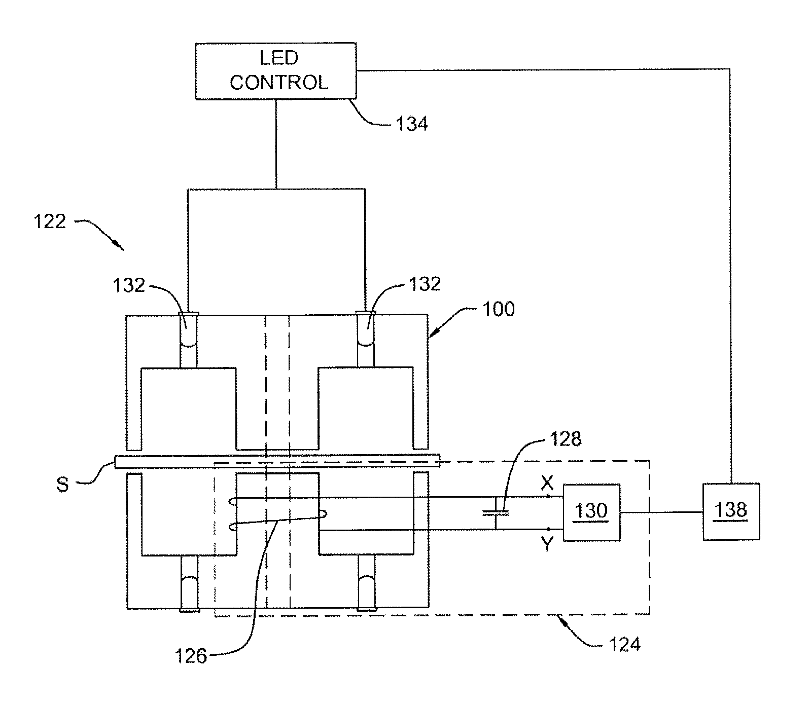
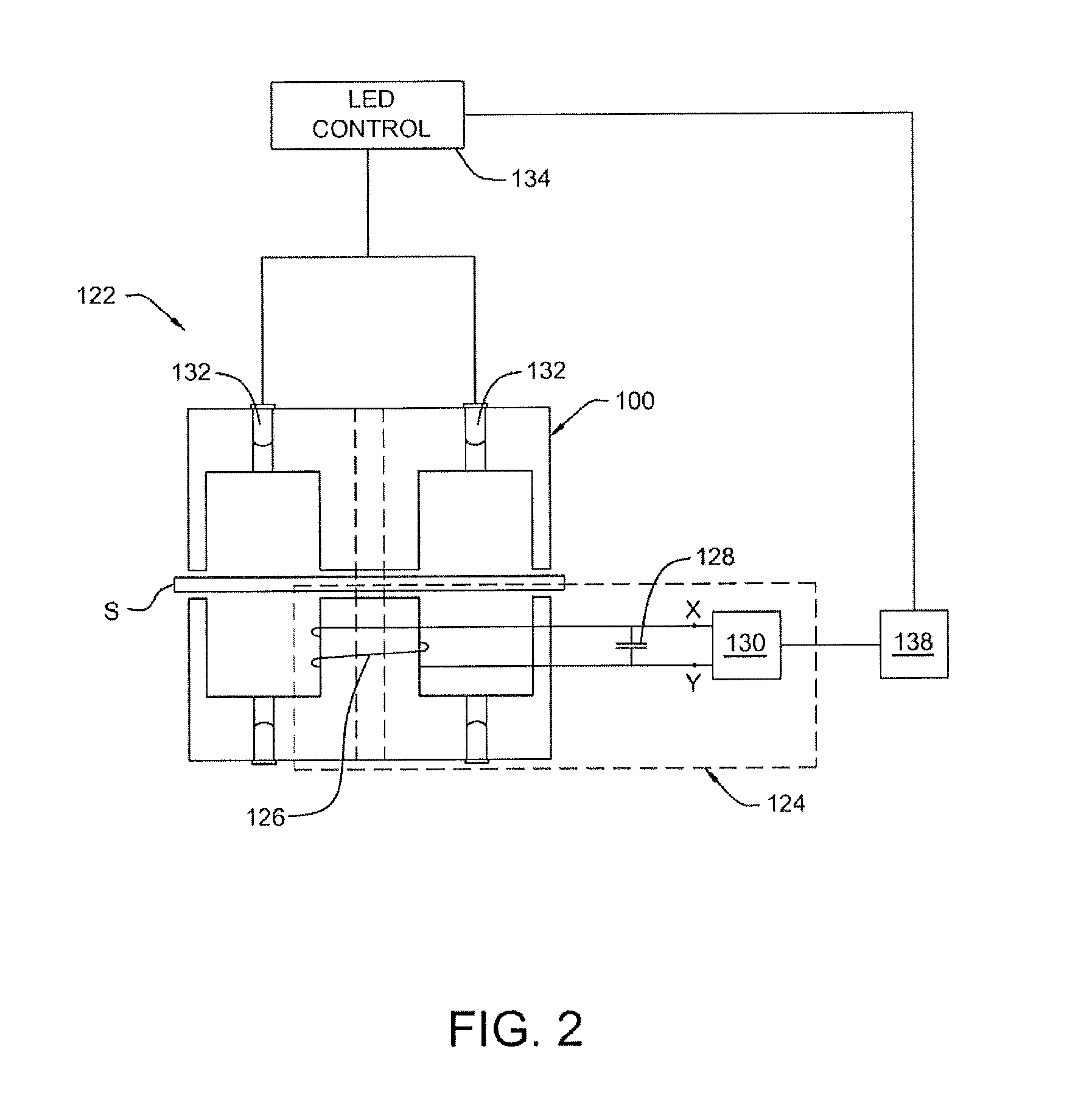
[0060]The present invention now will be described more fully hereinafter with reference to the accompanying drawings, in which some, but not all embodiments of the inventions are shown. Indeed, these inventions may be embodied in many different forms and should not be construed as limited to the embodiments set forth herein; rather, these embodiments are provided so that this disclosure will satisfy applicable legal requirements. Like numbers refer to like elements throughout.

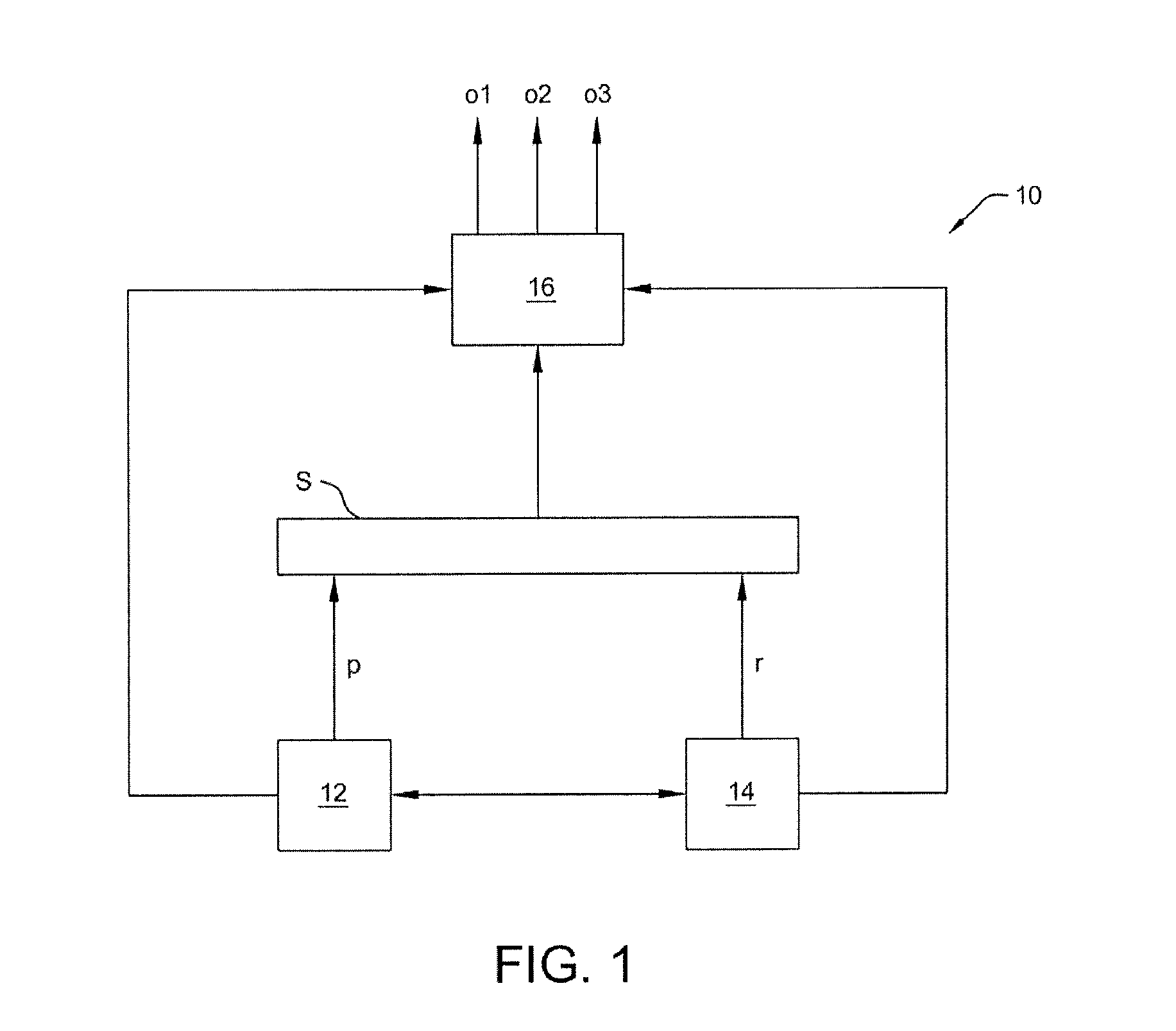
[0061]Referring to FIG. 1, therein is shown a schematic diagram of a system 10 for performing minority carrier lifetime measurements in a sample s of semiconductor material (“the sample”), the system being configured in accordance with an example embodiment. The system 10 includes a signal generation module 12 in communication with a radiation source module 14. As will be discussed further below, the signal generation module 12 acts to generate a probe signal p, for example, in the form of an oscillating electr...


PUM

PropertyMeasurementUnit
penetration depthaaaaaaaaaa

Abstract

A substrate is electromagnetically coupled into an inductance-capacitance resonant circuit formed from (i) a member comprising a ferromagnetic material, (ii) an inductor and (iii) the substrate. The substrate is illuminated for a first time period X to cause photoconduction in the substrate. Decay in conductivity of the substrate is monitored for a second time period Y. The ratio of X to Y is greater than 1:10. Bulk lifetime of the substrate is determined from the decay.

Description

CROSS-REFERENCE TO RELATED APPLICATIONS[0001]This application is a continuation-in-part of U.S. application Ser. No. 13 / 080,451 filed Apr. 5, 2011, which is a continuation-in-part of International Application No. PCT / US11 / 20783 filed Jan. 11, 2011, in the U.S. Receiving Office, which claims priority to U.S. application Ser. No. 12 / 687,855 filed Jan. 14, 2010. U.S. application Ser. No. 13 / 080,451 is also a continuation-in-part of U.S. application Ser. No. 12 / 687,855 filed Jan. 14, 2010. The disclosures of all applications are herein incorporated by reference in their entireties.FIELD OF THE INVENTION[0002]The invention relates generally to semiconductor characterization tools, and, more particularly, to apparatuses and methods for measuring bulk lifetime in a semiconductor sample.BACKGROUND[0003]Minority carrier lifetime is a quantity of fundamental importance for semiconductor materials. This quantity can provide an indication of the quality and defect density in raw semiconductor m...

Claims


Application Information

Patent Timeline
Patent Type & Authority Applications(United States)
IPC IPC(8): G01N27/02
CPCG01R31/2648H01L22/14G01R31/318511G01R31/2656
Inventor MACHUCA, FRANCISCOCHIARELLO, RONALDMILLER, G. LORIMERFOSTER, JOSEPH W.TIGWELL, DAVID C.CORNWELL, DAVID
Owner MKS INSTR INC
Learn More