Method for manufacturing semiconductor device and back-contact solar cell

Inactive Publication Date: 2012-12-06
TORAY IND INC
View PDF1 Cites 13 Cited by
  • Summary
  • Abstract
  • Description
  • Claims
  • Application Information

AI Technical Summary

Benefits of technology

[0022]On the other hand, according to the inkjet printing method described in Patent Literatures 4 and 5, breaking of a semiconductor substrate and the influence of scratches and contaminants can be avoided because an inkjet nozzle and the semiconductor substrate do not come into contact. However, a formed application pattern is, as shown in FIG. 5, a combined shape of a plurality of circles and patterning of a stripe shape with high precision is limited. Particularly in a semiconductor substrate having irregularities present on the back side, applied ink is likely to flow into a recess, making patterning with high precision more difficult.
[0023]Further, according to the technology disclosed by Patent Literatures 6 and 7, breaking of a semiconductor substrate and the influence of scratches and contaminants can be avoided because an application nozzle and the semiconductor substrate do not come into contact. Then, a solution is continuously ejected and so a stripe shape can be applied as a pattern. However, these technologies were developed mainly for the manufacture of liquid crystal display color filters. Thus, to realize a high-precision stripe application pattern, it is necessary to provide a bank called a black matrix between adjacent application patterns of different colors (RGB) so that such application patterns will not come into contact. A typical solution to be used for the manufacture of liquid crystal display color filters has a viscosity of about 10 mPa·s in an application nozzle orifice at room temperature and a typical boiling point of a solvent is at as high as about 200° C., the drying speed is slow, and the amount of application is relatively large (a typical thickness after drying is about 1 μm). Thus, the bank is generally further coated with a repellent so that application patterns will not come into contact. Therefore, when two or more different solutions are applied as patterns in a stripe shape, it is necessary to pattern the bank to partition such patterns by photolithography or coat the bank with a repellent in advance, which makes the simplification of processes not so promising even if the technology is applied to the manufacture of back-contact solar cells.
[0025]The present invention provides a manufacturing method capable of solving the above problems and reducing costs of a semiconductor device such as a back-contact solar cell by realizing high-precision pattern application with a smaller process number.
[0039]According to a manufacturing method of the present invention, a doping paste or the like can be applied as a pattern with high precision in a stripe shape and therefore, the manufacturing process of a semiconductor device such as back-contact solar cell can significantly be reduced and the reduction in cost can be realized. Also according to an embodiment of the manufacturing method of the present invention, the application method is a contactless method and thus, a high-performance semiconductor device (for example, a high conversion efficiency solar cell) can be provided without adversely affecting a semiconductor substrate. Further, according to an embodiment of a back-contact solar cell of the present invention, n-type and p-type doped regions are linearly shaped with precision even if random tiny irregularities are present on a surface on which doped regions of the semiconductor substrate are formed. Therefore, characteristics variations of the pn junction decrease so that reliability of the solar cell can greatly be improved.

Problems solved by technology

The method of repeatedly applying photolithography with many processes described above has a problem of increasing manufacturing costs of solar cells.
According to the technology in Patent Literature 1, n-type and p-type dopants can be diffused simultaneously, but the whole process is still very long.
Thus, if an attempt is made to pattern the diffusion mask 21 by photolithography on the back side of the semiconductor substrate 11, the following problems arise when a negative type photoresist 51 used for the patterning is exposed and developed via a photomask 57:(a) Unevenness of exposure of the photoresist is likely to arise because the angle of bottom reflection of exposure changes due to irregularities.(b) If the exposure is not sufficient, the photoresist cannot be patterned with high precision because a bottom 54 of the photoresist in a recess tends to be more likely to be developed (eroded).
Further, semiconductor substrates have been demanded to be thinner to reduce costs in recent years, but a thinner semiconductor substrate leads to less strength, making the semiconductor substrate more likely to be broken when a printing plate comes into contact .
Thus, the position of the opening is error-prone and it is difficult to reach the precision of pattern application of ±5 μm.
In addition, when, for example, n-type and p-type doping pastes are printed, unless contact resistance to the screen plate is made complete by first applying one paste and then solidifying the paste, the other paste cannot be printed.
However, a formed application pattern is, as shown in FIG. 5, a combined shape of a plurality of circles and patterning of a stripe shape with high precision is limited.
Particularly in a semiconductor substrate having irregularities present on the back side, applied ink is likely to flow into a recess, making patterning with high precision more difficult.

Method used


Image

  • Method for manufacturing semiconductor device and back-contact solar cell
  • Method for manufacturing semiconductor device and back-contact solar cell
  • Method for manufacturing semiconductor device and back-contact solar cell

Examples


example 1

Manufacturing Method of Forming a Solid-Phase Dopant Source With Clearance

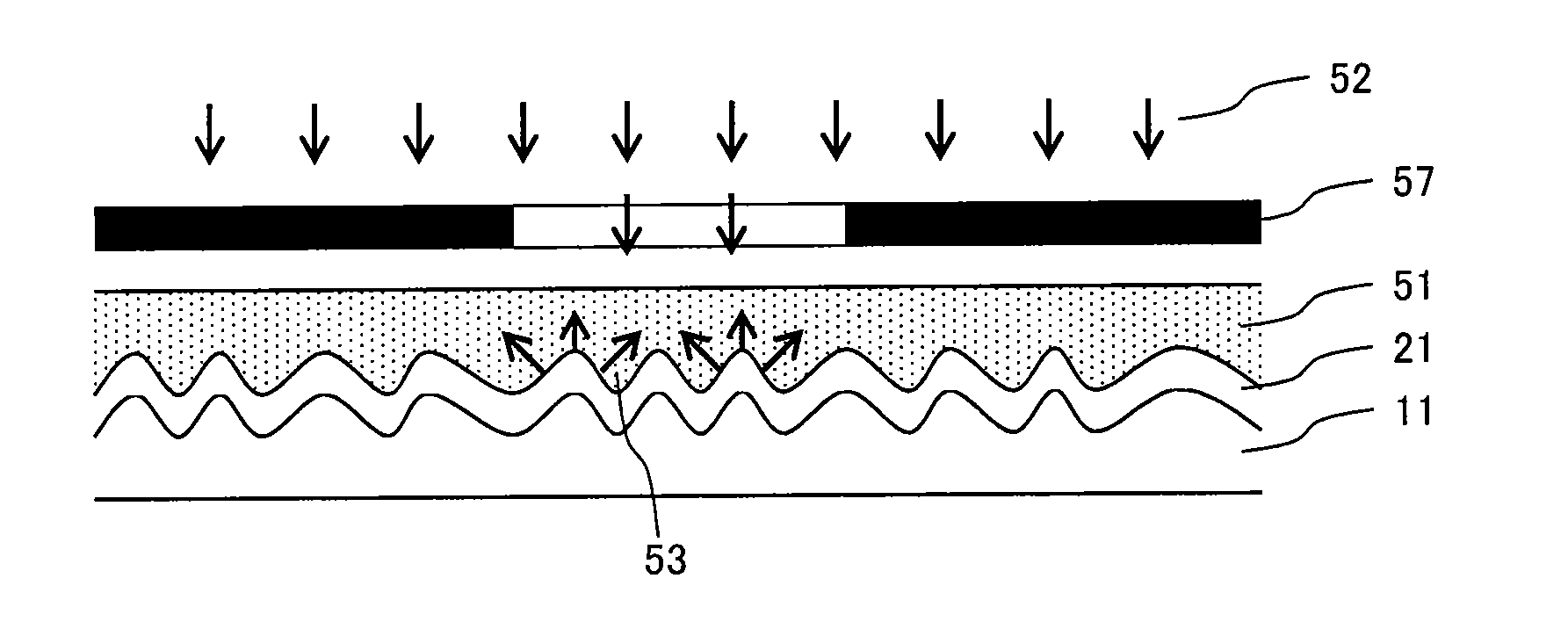
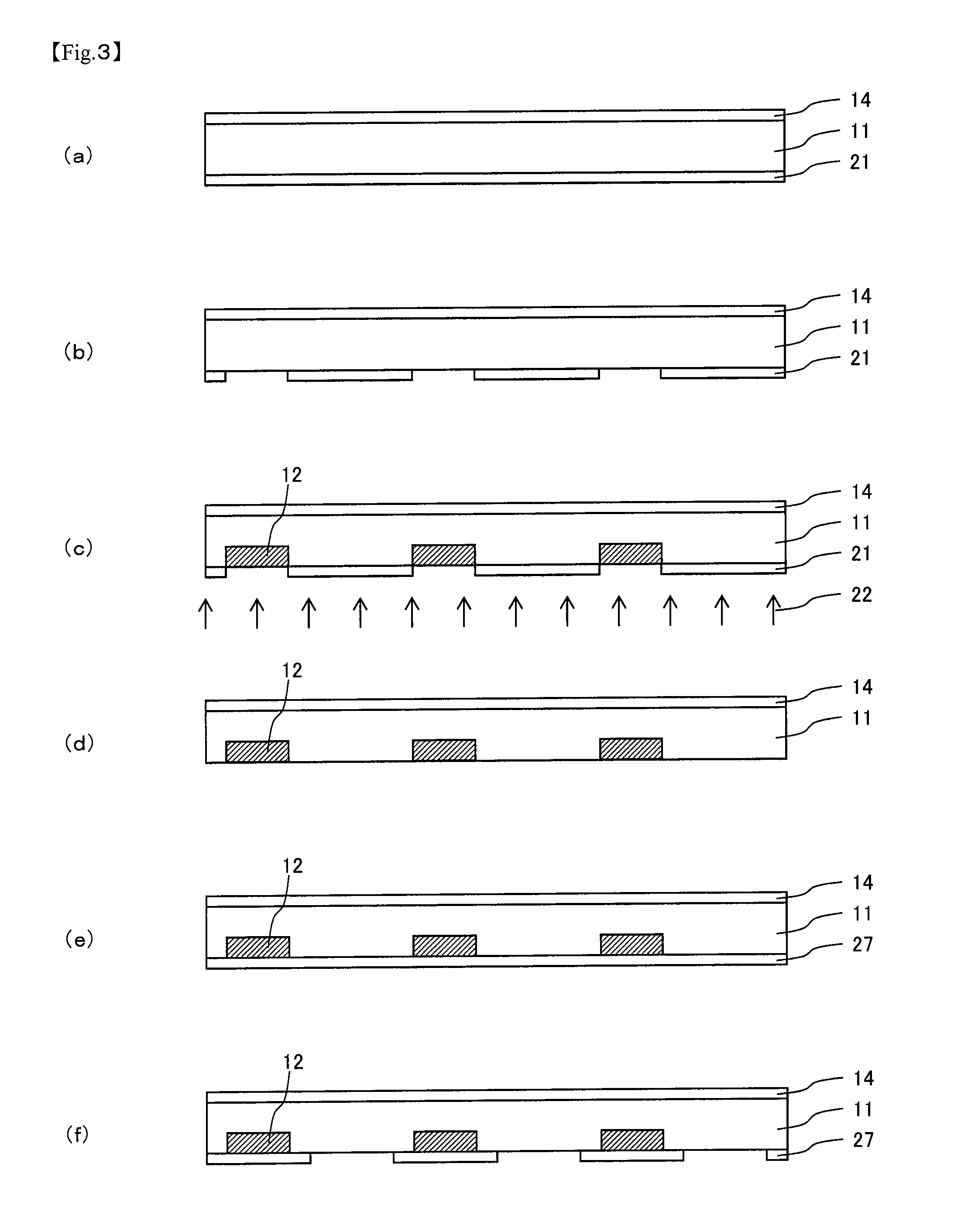
[0134]A back-contact solar cell was manufactured as described below based on the method shown in FIG. 6.

[0135]First, the semiconductor substrate 11 formed of n-type single crystalline silicon having the thickness of 250 μm and the length of one side of 100 mm was prepared and both surfaces thereof were etched by about 20 μm by a sodium hydrate solution and polished after water washing to remove slice damage and naturally-grown oxide.

[0136]Subsequently, (a) the passivation layer 14 having the thickness of 0.3 μm and formed of silicon nitride was formed on the light receiving side of the silicon substrate 11 by the plasma CVD method.

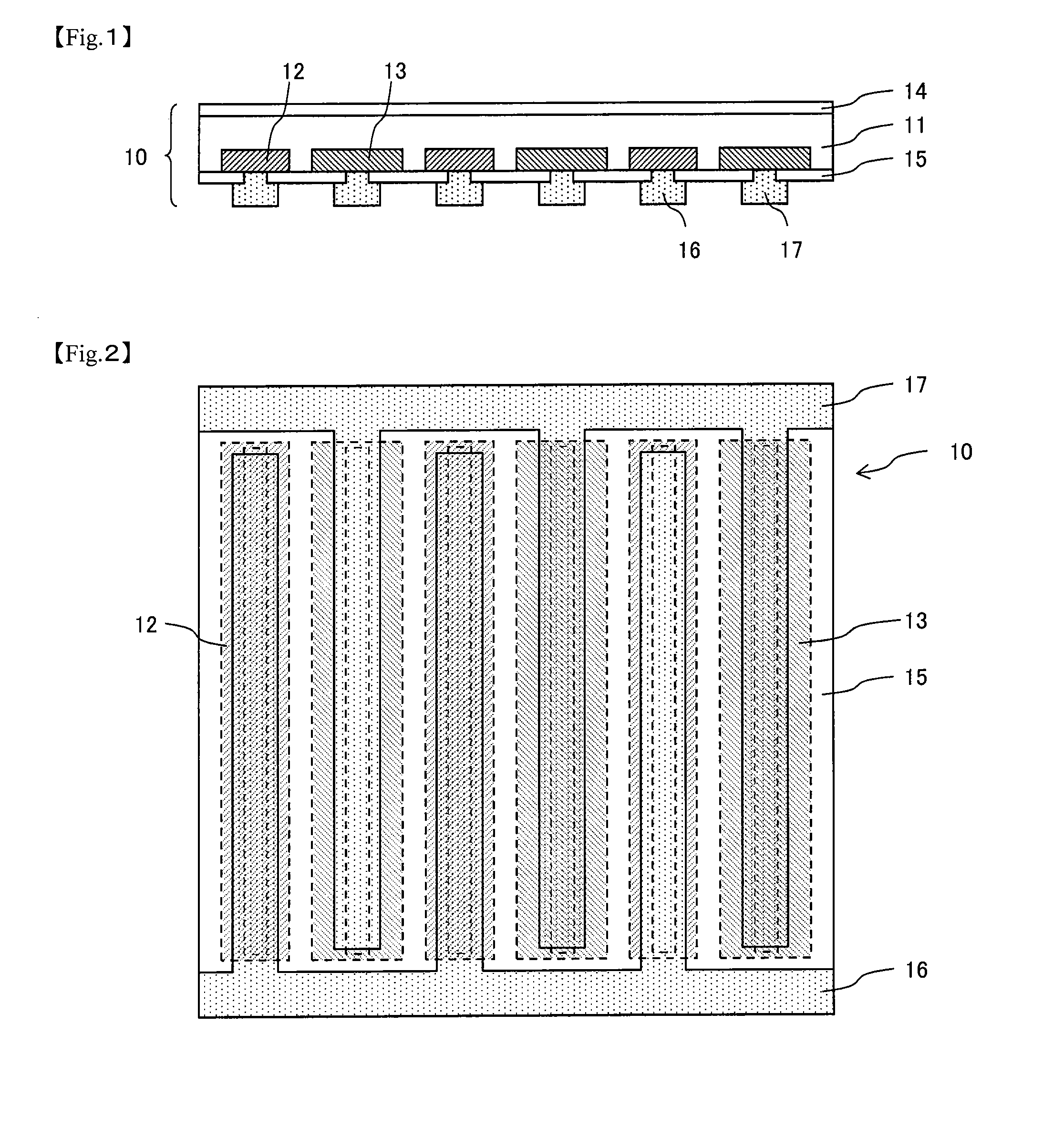
[0137]On the other hand, (b) an n-type doping paste was applied to the application surface (surface on the opposite side of the light receiving side) of the semiconductor substrate 11 in a stripe shape. Then, the n-type doping paste was heated at 150° C. for 30 min in the air and the...

example 2

[0148]The back-contact solar cell 10 was manufactured in the same manner as in Example 1 except that a mixed solution of 50 wt % of propylene glycol propyl ether (boiling point: 150° C.), 35 wt % of isopropyl alcohol, and 15 wt %) of ethyl acetate was used as the solvent of both doping pastes. The measurement of the shape of the n-type region 12 and the p-type region 13 in the same manner as in Example 1 showed that the interval between the n-type region 12 and the p-type region 13 was within a desired value ±8 μm in any measured region. The withstand voltage when a reverse bias was applied to a pn junction was also within the standard range and the back-contact solar cell 10 the same as in Example 1 was able to be manufactured. The amount of dry matter deposited at the nozzle tip was very small in long-time stripe application and the frequency of dry matter removal was significantly decreased when compared with Example 1.

example 3

[0149]The back-contact solar cell 10 was manufactured in the same manner as in Example 1 except that a mixed solution of 50 wt % of γBL (boiling point: 203° C.), 35 wt % of isopropyl alcohol, and 15 wt % of ethyl acetate was used as the solvent of both doping pastes. The measurement of the shape of the n-type region 12 and the p-type region 13 in the same manner as in Example 1 showed that the interval between the n-type region 12 and the p-type region 13 was within a desired value ±8 μm in any measured region. The withstand voltage when a reverse bias was applied to a pn junction was also within the standard range and the back-contact solar cell 10 the same as in Example 1 was able to be manufactured. No dry matter was deposited at the nozzle tip in long-time stripe application.


PUM


Abstract

A method is provided for manufacturing a semiconductor device, wherein a p-type region and / or n-type pattern is formed on a surface of a semiconductor substrate, including ejecting at least one of etching paste, masking paste, doping paste, and electrode paste from an ejecting orifice of a nozzle toward the surface of the semiconductor substrate to form beads formed of the paste between the semiconductor substrate and the ejecting orifice and moving the semiconductor substrate relative to the nozzle thereby the paste is applied to the surface of the semiconductor substrate in a stripe shape.

Description

CROSS-REFERENCE TO RELATED APPLICATIONS[0001]This application is the U.S. National Phase application of PCT International Application No. PCT / JP2010 / 072100, filed Dec. 9, 2010, and claims priority to Japanese Patent Application No. 2009-287155, filed Dec. 18, 2009, the disclosures of which PCT and priority applications are incorporated herein by reference in their entireties for all purposes.FIELD OF THE INVENTION[0002]The present invention relates to a method for manufacturing a semiconductor device and to a back-contact solar cell. In particular, the present invention relates to a suitable method for forming a stripe-shaped n-type or p-type doped region in a back-contact solar cell with high precision at low cost.BACKGROUND OF THE INVENTION[0003]A back-contact solar cell having no electrode on a light receiving side thereof can in principle expect high conversion efficiency and also features excellent architectural designs viewed from the light receiving side, and its practical us...

Claims


Application Information

Patent Timeline
IPC IPC(8): H01L31/18H01L31/0236H01L31/0224
CPCH01L31/022441Y02E10/547H01L31/1804H01L31/0682Y02P70/50H01L31/04H01L31/18
Inventor FUJIMORI, SHIGEOKITAMURA, YOSHIYUKIANDO, TAKASHIGOTO, TETSUYA
Owner TORAY IND INC
Why Eureka
Try Eureka