
Single-layer and multilayer graphene, method of manufacturing the same, object including the same, and electric device including the same

a single-layer, multi-layer technology, applied in the field of single-layer and multi-layer graphene, can solve the problems of difficult to form graphene on a complex curved surface or uneven object, and achieve the effects of high discharge capacity, high density, and large surface area of cathod

Active Publication Date: 2012-12-06
SEMICON ENERGY LAB CO LTD
View PDF6 Cites 65 Cited by
  • Summary
  • Abstract
  • Description
  • Claims
  • Application Information

AI Technical Summary

Benefits of technology

[0014]Another object of one embodiment of the present invention is to provide an electric device, particularly a cathode material or a power storage device with high capacity and less deterioration due to charging and discharging, including a graphene layer over an uneven object. Another object of one embodiment of the present invention is to provide a cathode material or a power storage device suitable for high-speed charging or extraction of high power. One embodiment of the present invention achieves at least one of the objects.
[0031]Further, the large surface area is preferable for lithium ions to move in and out at high speed, and high-speed charging and extraction of high power become possible.

Problems solved by technology

However, it is difficult to form graphene on a complex curved surface or an uneven object.

Method used


Image

  • Single-layer and multilayer graphene, method of manufacturing the same, object including the same, and electric device including the same
  • Single-layer and multilayer graphene, method of manufacturing the same, object including the same, and electric device including the same
  • Single-layer and multilayer graphene, method of manufacturing the same, object including the same, and electric device including the same

Examples


embodiment 1

[0045]In this embodiment, a method of forming graphene on an object will be described. Graphene oxide is obtained in such a manner that graphite is oxidized to form graphite oxide and the graphite oxide is subjected to ultrasonic vibrations. Patent Document 3 may be referred to for the details. Alternatively, commercial graphene oxide may be used.

[0046]Graphene oxide is dispersed in a solvent such as water or N-methylpyrrolidone (NMP). The solvent is preferably a polar solvent. The graphene oxide may be contained at a concentration of 0.1 g to 10 g per liter.

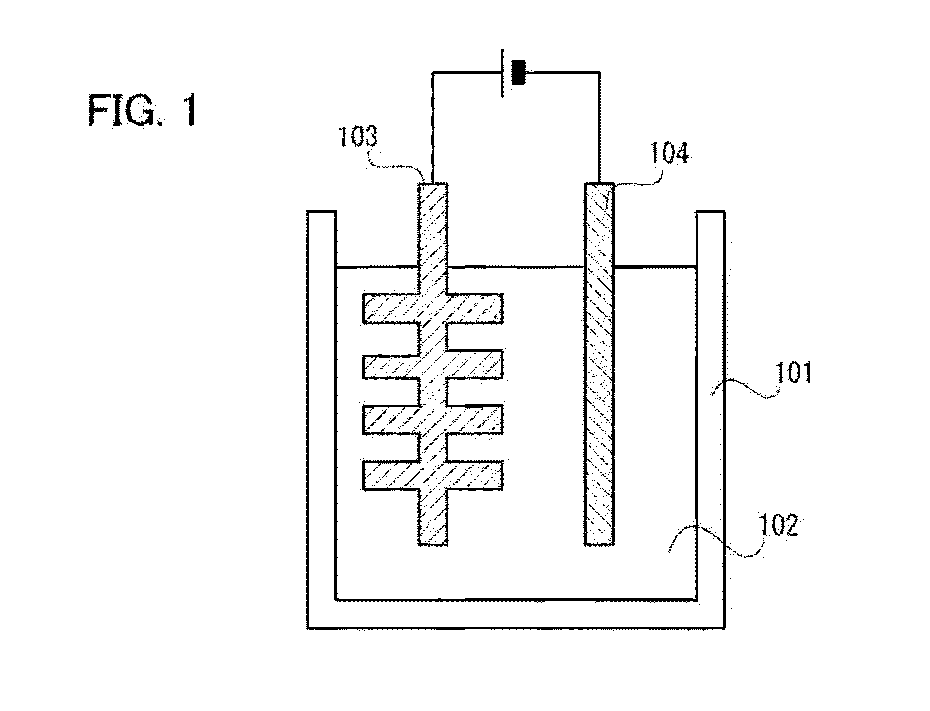
[0047]FIG. 1 illustrates an apparatus used in this embodiment. A solution 102 in which graphene oxide is dispersed is put in a container 101, and an object 103 on which a graphene layer is to be formed is put therein and is used as an anode. In addition, a conductor 104 serving as a cathode is put in the solution, and appropriate voltage (e.g., 5 V to 20 V) is applied between the anode and the cathode. Note that the voltage is n...

embodiment 2

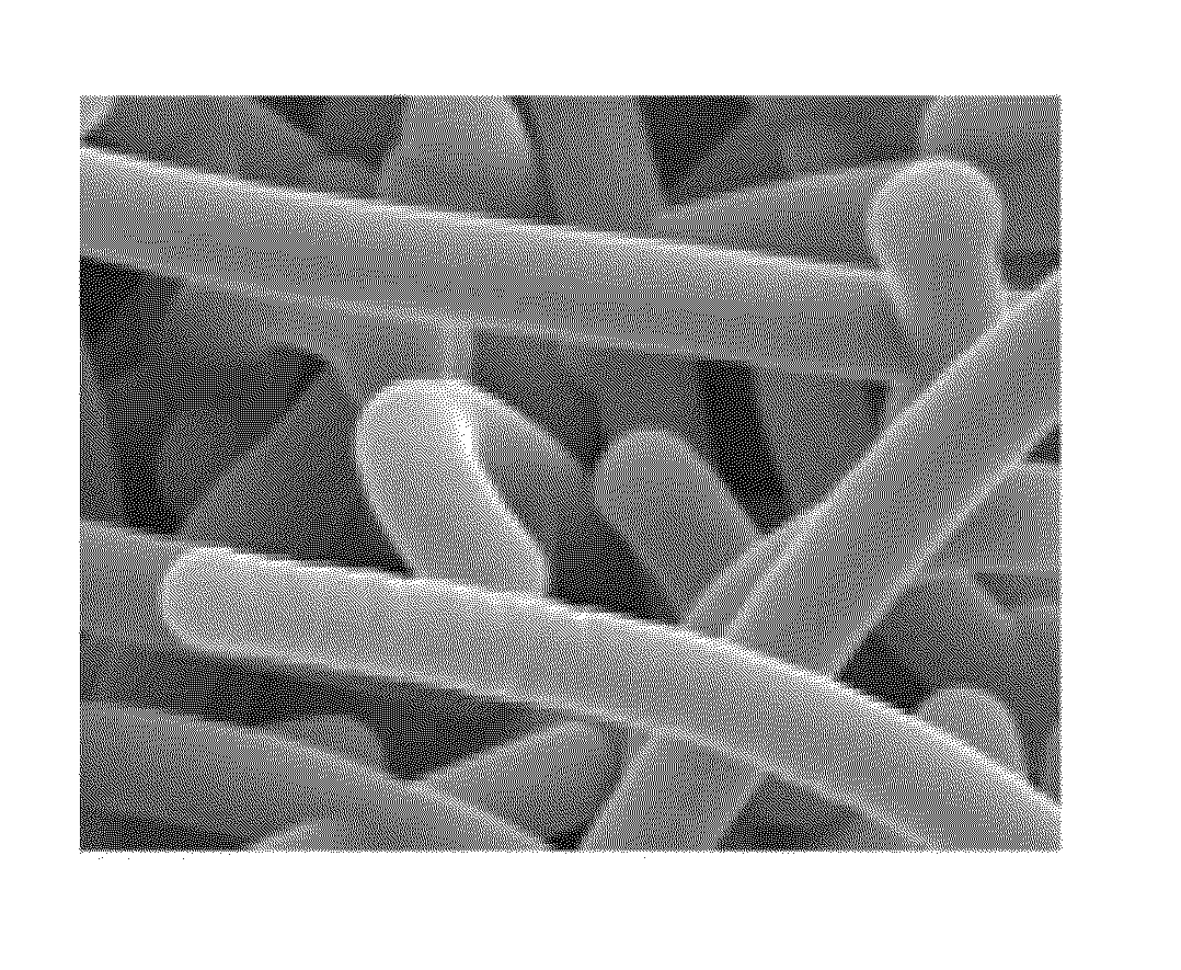
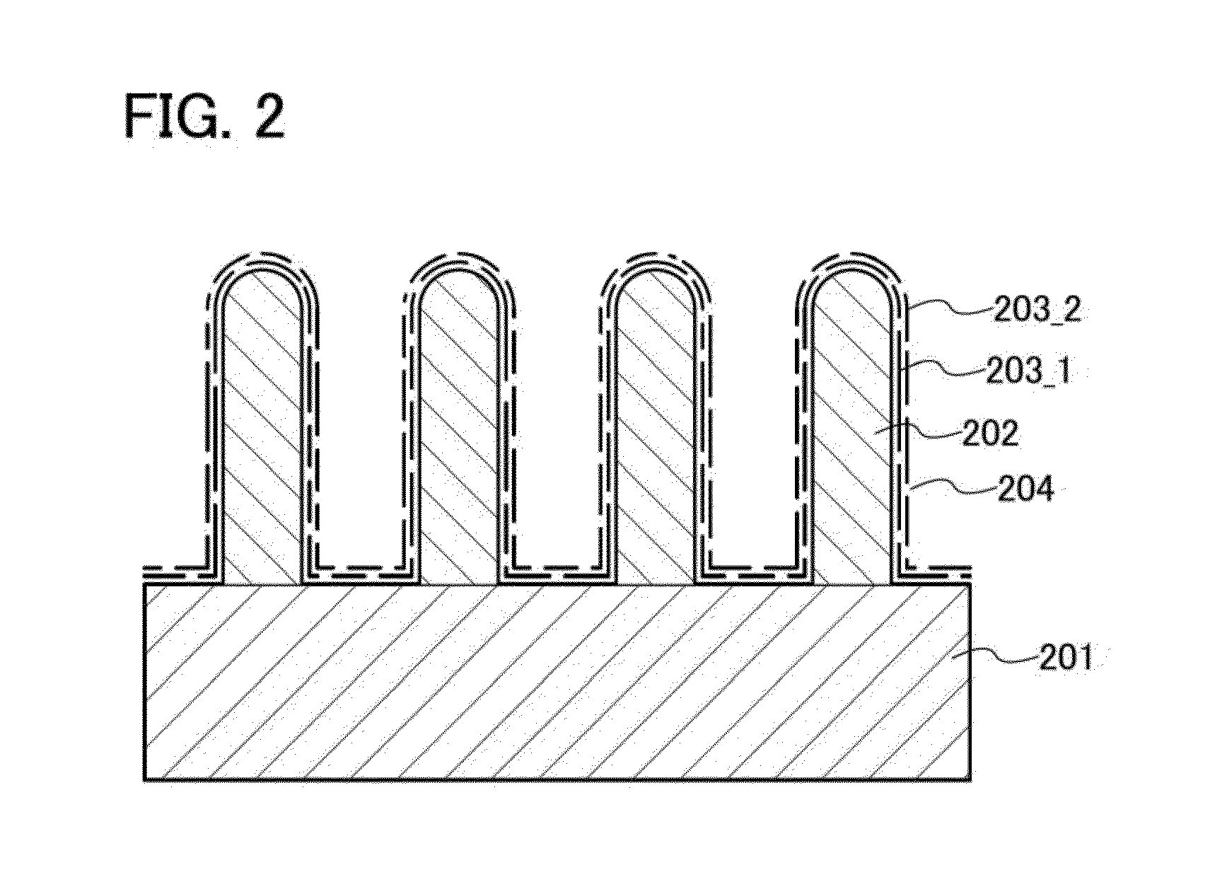
[0051]In this embodiment, an example in which 1 to 50 layers of graphene are formed on surfaces of silicon whiskers formed on one surface of a negative electrode current collector of a lithium-ion secondary battery will be described. In this embodiment, graphene is formed by an immersion method.

[0052]First, graphite is oxidized to form graphite oxide, and the graphite oxide is subjected to ultrasonic vibrations to obtain graphene oxide. The graphene oxide is dispersed in a solvent such as water or NMP.

[0053]A current collector with a silicon active material layer including silicon whiskers is immersed in the solution, taken out of the solution, and then dried. In addition, the current collector is heated at 150° C. or higher, preferably 200° C. or higher, in vacuum or a reducing atmosphere such as an inert gas (e.g., nitrogen or a rare gas) atmosphere. Through the above steps, 1 to 50 layers of graphene can be formed on a surface of the silicon active material layer.

[0054]The curren...

embodiment 3

[0068]In this embodiment, another example of forming a graphene layer including 1 to 50 layers of graphene on surfaces of whiskers formed over a current-collector will be described. In this embodiment, graphene is formed by an electrophoresis method. As in Embodiment 2, graphene oxide is dispersed in a solvent such as water or NMP. The graphene oxide may have a concentration of 0.1 g to 10 g per liter.

[0069]A current collector provided with whiskers is put in a solution in which graphene oxide is dispersed and is used as an anode. A conductor serving as a cathode is also put in the solution, and appropriate voltage (e.g., 5 V to 20 V) is applied between the anode and the cathode. Since part of an edge of a graphene sheet with a certain size in graphene oxide is terminated with a carboxyl group (—COOH), hydrogen ions detach from the carboxyl group in a solvent such as water and the graphene oxide itself is negatively charged. Thus, the graphene oxide is drawn to and deposited on an a...


PUM

PropertyMeasurementUnit
lengthaaaaaaaaaa
concentrationaaaaaaaaaa
voltageaaaaaaaaaa

Abstract

Graphene is formed with a practically uniform thickness on an uneven object. The object is immersed in a graphene oxide solution, and then taken out of the solution and dried; alternatively, the object and an electrode are immersed therein and voltage is applied between the electrode and the object used as an anode. Graphene oxide is negatively charged, and thus is drawn to and deposited on a surface of the object, with a practically uniform thickness. After that, the object is heated in vacuum or a reducing atmosphere, so that the graphene oxide is reduced to be graphene. In this manner, a graphene layer with a practically uniform thickness can be formed even on a surface of the uneven object.

Description

BACKGROUND OF THE INVENTION[0001]1. Field of the Invention[0002]The present invention relates to single-layer graphene which is a one-atom-thick sheet of carbon molecules having sp2 bonds, multilayer graphene in which 2 to 100 layers, preferably 2 to 50 layers, more preferably 2 to 20 layers of the single-layer graphene are stacked, a method of manufacturing the single-layer or multilayer graphene, and an electric device (power storage device) including the single-layer or multilayer graphene.[0003]In this specification, single-layer graphene and multilayer graphene are simply collectively referred to as graphene (or graphene layer). When the number of layers of graphene is specified as x, the graphene is referred to as “x layers of graphene.” Note that graphene is also two-dimensionally extended polyacene (see Patent Document 5).[0004]2. Description of the Related Art[0005]Graphene has excellent electrical characteristics such as high conductivity and high mobility and excellent ph...

Claims


Application Information

Patent Timeline
Patent Type & Authority Applications(United States)
IPC IPC(8): B32B3/00C25D13/12H01M4/13C25D13/00B82Y30/00B82Y40/00
CPCB82Y30/00Y10T428/24355H01M4/66H01M4/587H01M4/1393H01M4/133Y02E60/122H01M4/0452C25D13/12C25D13/02C25D5/50C25D5/48B82Y40/00H01M4/0471H01M4/70Y02E60/10B32B3/30H01B1/04H01M4/583C01B32/194C01B32/198H01M4/0428
Inventor OGUNI, TEPPEIOSADA, TAKESHITAKEUCHI, TOSHIHIKONOMOTO, KUNIHARU
Owner SEMICON ENERGY LAB CO LTD
Learn More