Packaged chip for multiplexing photonic crystal waveguide and photonic crystal slot waveguide devices for chip-integrated label-free detection and absorption spectroscopy with high throughput, sensitivity, and specificity

a technology of photonic crystal waveguide and integrated optical device, which is applied in the field of package chip integrated optical device, chip-integrated infrared optical absorption spectroscopy, can solve the problems of small wavelength range over which light is slowed down as it propagates down the photonic crystal waveguide, and achieve efficient light coupler, increase measurement throughput, and maximum efficiency

Active Publication Date: 2013-01-03
OMEGA OPTICS
View PDF2 Cites 56 Cited by
  • Summary
  • Abstract
  • Description
  • Claims
  • Application Information

AI Technical Summary

Benefits of technology

[0016]The semiconductor chip comprising the substrate, the bottom cladding, the slab with the device elements, the cover polymer, and the rigid dielectric layer are placed in a package made of ceramic or plastic. The package has holes that allow the optical fibers or the external light source to interface with the sub-wavelength grating couplers. The rectangular ceramic package is patterned at the four corners with grooves that enable precision positioning of the semiconductor chip with the external measurement setup containing the external input and output optical fibers. The input and output optical fibers in the external measurement setup are precisely aligned to deliver and collect light respectively at maximum efficiency from the input and output sub-wavelength grating couplers.
[0017]The primary objective of the invention is to provide a

Problems solved by technology

However, in a photonic crystal slot waveguide, the wavelength range over which light is slowed down as it propagates down the photonic crystal waveguide is small.
The was

Method used


Image

  • Packaged chip for multiplexing photonic crystal waveguide and photonic crystal slot waveguide devices for chip-integrated label-free detection and absorption spectroscopy with high throughput, sensitivity, and specificity
  • Packaged chip for multiplexing photonic crystal waveguide and photonic crystal slot waveguide devices for chip-integrated label-free detection and absorption spectroscopy with high throughput, sensitivity, and specificity
  • Packaged chip for multiplexing photonic crystal waveguide and photonic crystal slot waveguide devices for chip-integrated label-free detection and absorption spectroscopy with high throughput, sensitivity, and specificity

Examples


second embodiment

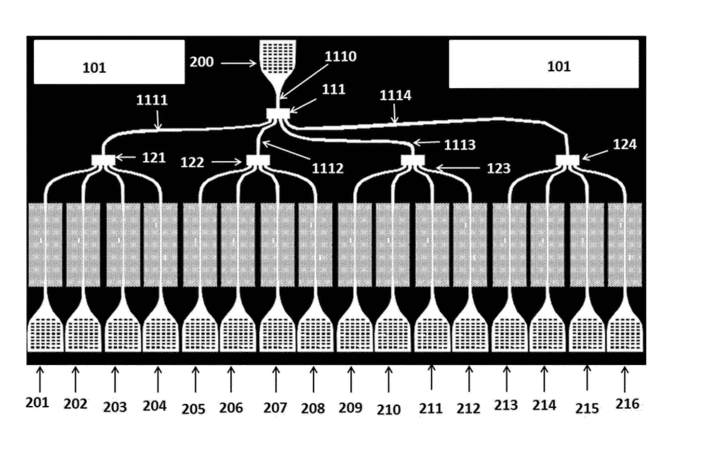
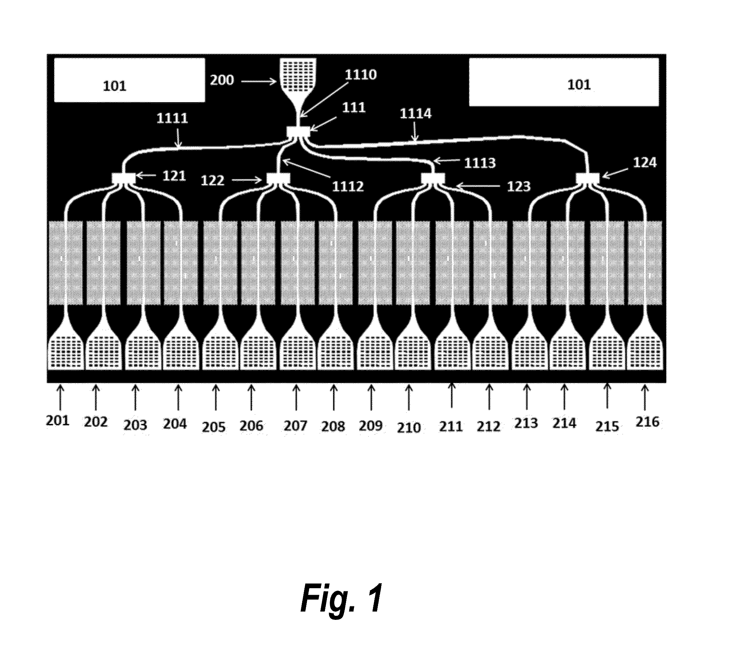
[0086]FIG. 18 is the top view of the packaged optical chip showing the layout of the chip in FIG. 1 or FIG. 12 in the package 600. Square grooves 601, 602, 603, and 604 are made at the four corners of the package. The package 600 may be ceramic, plastic, or any material which provides toughness and environmental protection to the internal semiconductor chip. The opening in the package 701 on the top side is aligned with the microfluidic channel opening 700 in the semiconductor chip. Openings are made in the package 600 as bordered by the segments 1071 and 1072. The element 109 is also voided in the region bordered by 1071 and 1072 so that the element 108 is exposed. In essence, light is then coupled into the semiconductor chip from the top of the chip from external optical sources and through the top cover polymer cover 108. Similarly, light is coupled out of the semiconductor chip from the top of the chip to external optical detectors and through the top cover polymer cover 108.

[00...

third embodiment

[0088]FIG. 20 is the top view of the packaged optical chip showing the layout of the chip in FIG. 1 or FIG. 12 in the package 600. Square grooves 601, 602, 603, and 604 are made at the four corners of the package. The package 600 may be ceramic, plastic, or any material which provides toughness and environmental protection to the internal semiconductor chip. The opening in the package 701 on the top side is aligned with the microfluidic channel opening 700 in the semiconductor chip. Openings are made in the package 600 as bordered by the segments 1071 and 1072. The elements 108 and 109 are also voided in the region bordered by 1071 and 1072 so that the input sub-wavelength grating coupler 200 and the output sub-wavelength grating couplers 201, 202, 203 . . . 216 are exposed. In essence, light is then coupled into the semiconductor chip from the top of the chip from external optical sources and directly into the input sub-wavelength grating coupler 200. Similarly, light is coupled ou...


PUM


Abstract

Systems and methods for chip-integrated label-free detection and absorption spectroscopy with high throughput, sensitivity, and specificity are disclosed. The invention comprises packaged chips for multiplexing photonic crystal waveguide and photonic crystal slot waveguide devices. Other embodiments are described and claimed.

Description

BACKGROUND[0001]1. Field of the Invention[0002]This invention relates generally to the field of packaged chip integrated optical devices, for chip-integrated infrared optical absorption spectroscopy as well as chip-integrated label-free biomolecule microarray. The apparatus and method enables high throughput sensing as well as high specificity.[0003]2. Background of the Invention[0004]Label-free biosensors are particularly attractive since they avoid complex chemistries caused by steric hindrance of the labels. All methods of detection in lab-on-chip platforms at present transduce the specific binding of the biomolecule of interest to its specific conjugate biomolecule receptor bound to the device substrate, into an electrical, mechanical, or optical signal. Optical detection techniques are generally preferred due to their freedom from electromagnetic interference. While several platforms based on ring resonators, wire waveguides, and surface plasmon resonance (SPR) have been invest...

Claims


Application Information

Patent Timeline
IPC IPC(8): C40B30/04G02B6/00G01J3/42C40B60/12
CPCG01N21/253G01N33/54373G01N21/255G01N2021/7789G02B6/1225G01N21/7746
Inventor CHAKRAVARTY, SWAPNAJITCHEN, RAY T.HOSSEINI, AMIR
Owner OMEGA OPTICS
Why Eureka
Try Eureka