Metal nanowires with high linearity, method for producing the metal nanowires and transparent conductive film including the metal nanowires

a technology of metal nanowires and linearity, applied in the direction of nanostructure manufacturing, non-conductive materials with dispersed conductive materials, nuclear engineering, etc., can solve the problems of high production cost of ito thin films, difficult to form ito thin films on highly flexible plastic substrates and films, and deterioration of their characteristics, etc., to achieve high linearity, low sheet resistance, and high transmittance

Active Publication Date: 2013-04-11
KOREA INST OF SCI & TECH
View PDF6 Cites 57 Cited by
  • Summary
  • Abstract
  • Description
  • Claims
  • Application Information

AI Technical Summary

Benefits of technology

[0038]According to the present invention, the metal nanowires have high linearity and can be produced using metal salts at a relatively low temperature. Particularly, according to the present invention, the metal nanowires can be used to form a transparent conductive film with high transmittance, low sheet resistance, and good thermal, chemical and mechanical stability. The transparent conductive film of the present invention has a high electrical conductivity due to the high linearity of the metal nanowires. In addition, the metal nanowires take up 5% or less of the volume of the tra

Problems solved by technology

However, since indium as a principal material of ITO is an expensive limited resource, a new transparent conducting material as a substitute for ITO is strongly needed.
This heating leads to high production costs of ITO thin films and makes it difficult to form ITO thin films on highly flexible plastic substrates and films.
Further, ITO films deposited on polymer films are not satisfactory in terms of flexibility and are readily degraded when exposed to plasma, resulting in deterioration of their characteristics.
However, a sheet resistance of 1 kΩ/sq. or less is generally not obtained in a 50 nm thick coating of a conductive polymer on a substrate.
That

Method used


Image

  • Metal nanowires with high linearity, method for producing the metal nanowires and transparent conductive film including the metal nanowires
  • Metal nanowires with high linearity, method for producing the metal nanowires and transparent conductive film including the metal nanowires
  • Metal nanowires with high linearity, method for producing the metal nanowires and transparent conductive film including the metal nanowires

Examples


example 1

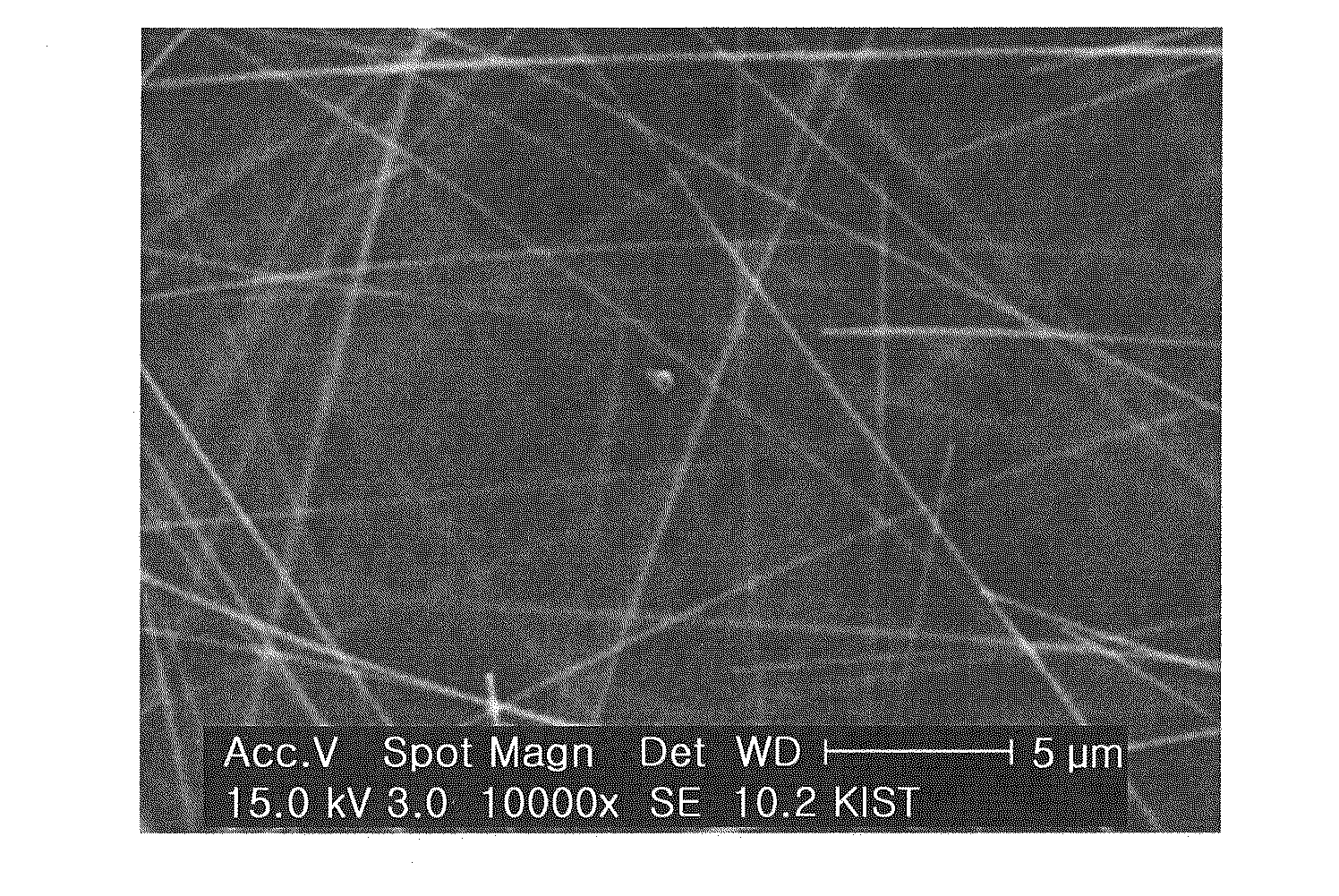
[0070]5-8 g of polyvinylpyrrolidone (PVP K-90) having a molecular weight between 900,000 and 1,500,000 was added to 200 ml of ethylene glycol (EG) in a round-bottom flask and slowly stirred in an oil bath. After the mixture was heated to a temperature of 170° C., 0.01-0.2 g of cetyltrimethylammonium bromide (CTBA) or potassium bromide (KBr) as a reducing agent was added thereto and was allowed to react with stirring for 40 min. To the reaction solution was added 0.5-1 g of silver chloride. The reaction was allowed to proceed. After addition of 1-3 g of silver nitrate, the reaction was allowed to proceed to produce Ag nanowires with high linearity. The Ag nanowires were found to have a diameter of 30 nm or less and a length of 40 μm or more.

[0071]FIG. 1 is a scanning electron microscopy (SEM) image of the Ag nanowires.

example 2

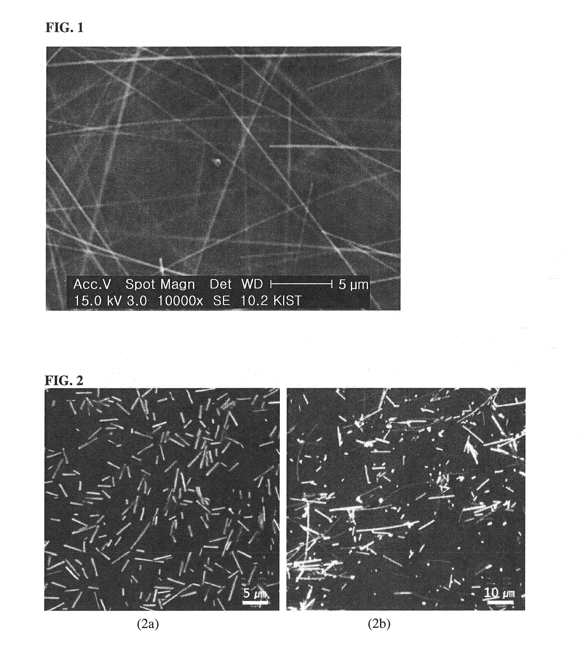
[0072]Two kinds of Ag nanowires were produced in the same manner as in Example 1, except that PVP having a molecular weight between 500,000 and 800,000 and PVP K-120 having a molecular weight between 2,000,000 and 3,000,000 were separately used. FIG. 2 shows scanning electron microscopy (SEM) images of the Ag nanowires produced using the PVP (2a) and the Ag nanowires produced using the PVP K-120 (2b). The SEM images confirm that it is more difficult to increase the diameter of the Ag nanowires when the polyvinylpyrrolidone having a lower molecular weight is used.

example 3

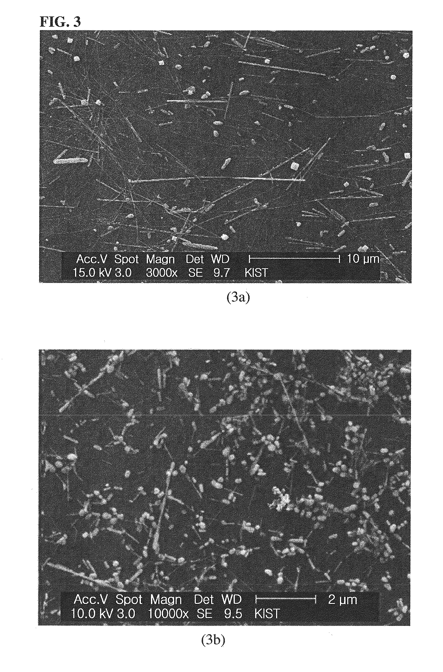
[0073]Ag nanowires were produced in the same manner as in Example 1, except that the cetyltrimethylammonium bromide (CTBA) or potassium bromide (KBr) was added in different amounts of 0.01-0.5 g.

[0074]FIG. 3 shows scanning electron microscopy (SEM) images of the Ag nanowires. Spherical Ag particles are observed, together with the Ag nanowires, in the SEM image (3b).


PUM

PropertyMeasurementUnit
Temperatureaaaaaaaaaa

Abstract

Metal nanowires with high linearity can be produced using metal salts at a relatively low temperature. A transparent conductive film can be formed using the metal nanowires. Particularly, the transparent conductive film has high transmittance, low sheet resistance, and good thermal, chemical and mechanical stability. The transparent conductive film has a high electrical conductivity due to the high linearity of the metal nanowires. The metal nanowires take up 5% or less of the volume of the transparent conductive film, ensuring high transmittance of the transparent conductive film. Furthermore, the metal nanowires are useful as replacements for existing conductive materials, such as ITO, conductive polymers, carbon nanotubes and graphene. The metal nanowires can be applied to flexible substrates and other various substrates due to their good adhesion and high applicability to the substrates. Moreover, the metal nanowires can find application in various fields, such as displays and solar cell devices.

Description

CROSS-REFERENCE TO RELATED APPLICATIONS[0001]This application claims priority under 35 U.S.C. §119 to Korean Patent Application No. 10-2011-0.103436 filed on Oct. 11, 2011, in the Korean Intellectual Property Office, the disclosure of which is incorporated herein by reference in its entirety.BACKGROUND OF THE INVENTION[0002]1. Field of the Invention[0003]The present invention relates to metal nanowires with high linearity and a transparent conductive film including the same. More specifically, the present invention relates to metal nanowires with high linearity that have excellent electrical properties and high transmittance; and a transparent conductive film that includes the metal nanowires and is thus suitable for use as a transparent electrode for a variety of electronic devices, including flexible electronics, and energy devices.[0004]2. Description of the Related Art[0005]Transparent conducting materials (TCMs) should exhibit a high transmittance (≧90%) in the visible waveleng...

Claims


Application Information

Patent Timeline
IPC IPC(8): H01B5/02B22F9/18C22C19/03C22C9/00B05D5/12B05D3/06H01B1/22C22C5/06B82B1/00B82B3/00B82Y30/00
CPCH01L31/022466H01L31/1884B82Y30/00C22C5/06C22C9/00Y02E10/50H01B1/02H01B1/026B22F1/0025B22F3/10B22F9/24C22C19/03B22F1/0547B82B3/00B82B1/00B82Y40/00
Inventor OH, YOUNG-JEIWANG, BYUNG-YONG
Owner KOREA INST OF SCI & TECH
Why Eureka
Try Eureka