Organic photoelectric conversion element and solar cell using same

Active Publication Date: 2013-04-25
KONICA MINOLTA INC
View PDF4 Cites 21 Cited by
  • Summary
  • Abstract
  • Description
  • Claims
  • Application Information

AI Technical Summary

Benefits of technology

[0053]According to the present invention, an organic photoelectric conversion element exhibiting a high photoelectric conversion efficienc

Problems solved by technology

However, the cost of electric power generation with these solar cells is still higher than the price of electricity generated and transmitted using the fossil fuel, and it has been an obstacle for the spread of solar cells.
Moreover, it has been needed to use a heavy glass as a substrate, and a reinforcement work has been required at the time of installation.
This has also been a cause which increases the cost of electric power generation.
However, the durability of an organic thin film solar battery is still insufficient, and the improvement is still expected.
However, in the reverse layer type organic thin film solar cell as disclosed by such as the above mentioned Patent Document 1 and Non-Patent document 2, the fill factor was as low as 0.52 which had been a problem to improve the efficiency.
Accordingly, a problem that the durability is low has been left unsolved.
Also, another problem has been left unresolved, namely

Method used


Image

  • Organic photoelectric conversion element and solar cell using same
  • Organic photoelectric conversion element and solar cell using same
  • Organic photoelectric conversion element and solar cell using same

Examples


Example

Example 1

[Preparation of Organic Photoelectric Conversion Element 1]

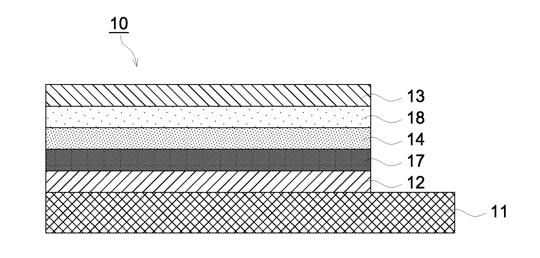
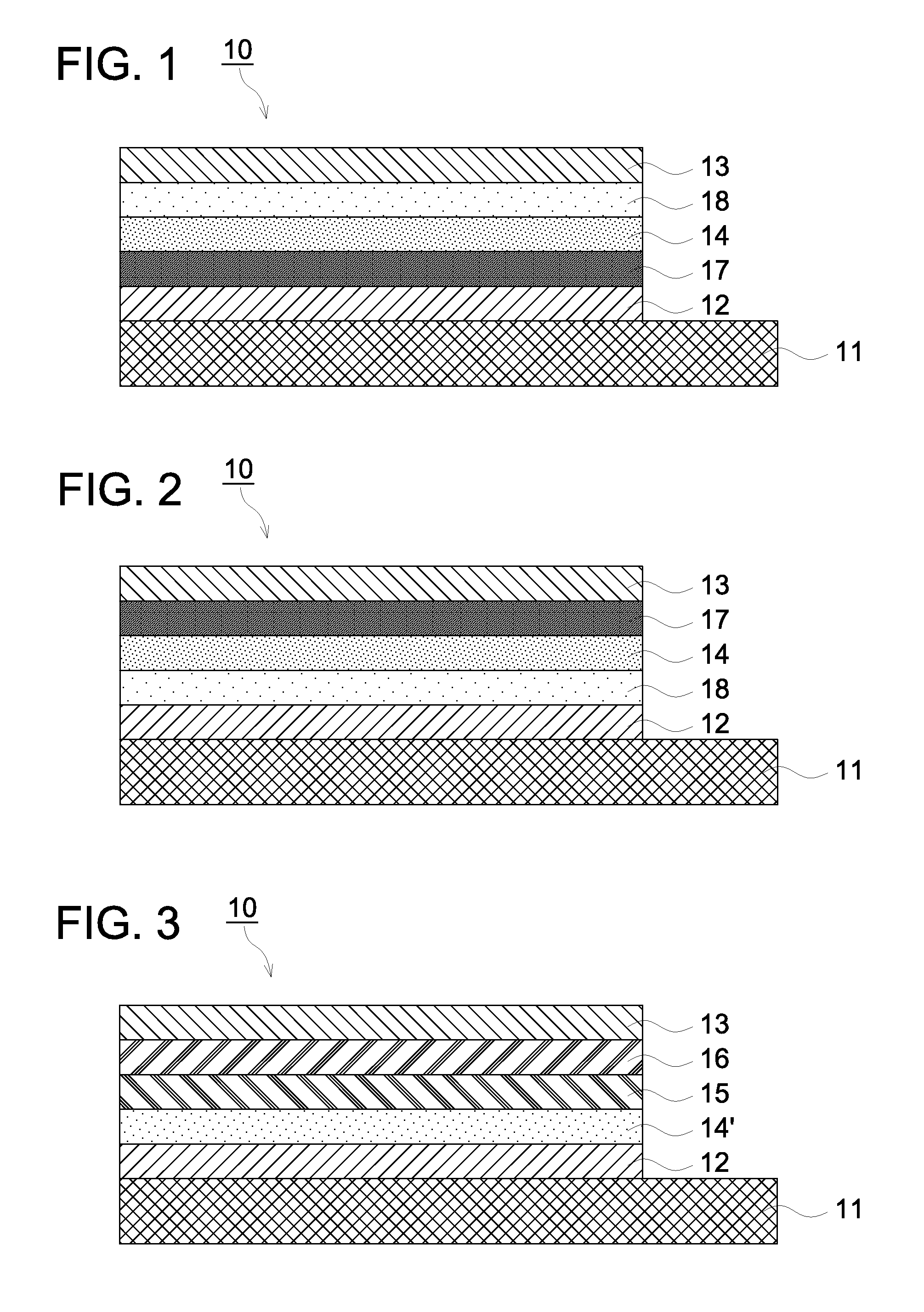
[0158]With referring to Non-Patent Document 4, Organic photoelectric conversion element 1 of a forward layer structure in which the n-type organic semiconductor material had a concentration gradient as prepared. Only in Organic photoelectric conversion element 1, the first electrode was used as the anode and the second electrode was used as the cathode.

(Formation of the First Electrode)

[0159]A transparent conductive film made of indium tin oxide (ITO) was deposited on a substrate composed of PEN to have a thickness of 150 nm. By using a usual photolithography technique and hydrochloric acid etching, a transparent electrode having a pattern of 2 mm width was formed to obtain an anode (the first electrode).

[0160]The aforementioned anode which had been subjected to pattern formation was successively cleaned by: ultrasonic cleaning using a surfactant and ultrapure water, and finally ultrasonic cleaning with ultrapure wa...

Example

Example 2

Evaluation of Formation of Hole Transport Layer on Photoelectric Conversion Layer

(Preparation of Organic Photoelectric Conversion Element 12″)

[0187]Organic photoelectric conversion element 12″ was prepared in the same manner as the preparation of Organic photoelectric conversion element 12 except that the coating of hole transport layer was carried out in a glove box (a nitrogen atmosphere in which oxygen concentration was 10 ppm or less and the dew point was −70° C. or lower), but not in an ambient atmosphere, via a gravure coating method which is more probable in a practical production process.

[0188]However, in the extremely dried atmosphere in the glove box, the aqueous solvent in the hole transport layer was repelled and film formation of S three sheets among prepared 5 sheets of organic photoelectric conversion element were unsuccessful.

(Preparation of Organic Photoelectric Conversion Element 15″)

[0189]Organic photoelectric conversion element 15″ was prepared in the sa...


PUM

PropertyMeasurementUnit
Fractionaaaaaaaaaa
Fractionaaaaaaaaaa
Fractionaaaaaaaaaa

Abstract

Disclosed is an organic photoelectric conversion element which has a reverse layer structure wherein at least a first electrode, a photoelectric conversion layer and a second electrode are arranged on a substrate in this order. The organic photoelectric conversion element is characterized in that: the photoelectric conversion layer is a bulk heterojunction layer that is composed of a p-type organic semiconductor material and an n-type organic semiconductor material; and a compound that has a linear or branched fluorinated alkyl group having 6-20 carbon atoms is contained as the p-type organic semiconductor material.

Description

TECHNICAL FIELD[0001]The present invention relates to an organic photoelectric conversion element and a solar cell, and, in more detail, relates to a bulk heterojunction-type organic photoelectric conversion element and a solar cell employing this organic photoelectric conversion element.BACKGROUND[0002]Due to the steep rise of fossil energy price in recent years, required has been the system which can generate electric power directly from natural energy. To respond such requirement, it has been proposed or put to practical use a solar cell using Si in a single crystal, a polycrystalline state, or an amorphous state, a solar cell made of a compound of GaAs or CIGS (namely, a semiconductor material containing copper (Cu), indium (In), gallium (Ga) and Selenium (Se)), or a dye sensitized photoelectric conversion element (Gratzel cell).[0003]However, the cost of electric power generation with these solar cells is still higher than the price of electricity generated and transmitted usin...

Claims


Application Information

Patent Timeline
IPC IPC(8): H01L51/00
CPCB82Y10/00H01L51/002H01L51/0036H01L51/0047Y02E10/549H01L51/4253H01L51/0072H01L51/0043H01L51/0094H10K71/30H10K85/113H10K85/151H10K85/215H10K85/40H10K30/30H10K30/50H10K85/6572
Inventor OKUBO, YASUSHITANI, KUNIO
Owner KONICA MINOLTA INC
Why Eureka
Try Eureka