Flexible electronic device, method for manufacturing same, and a flexible substrate

a flexible electronic and substrate technology, applied in the direction of organic semiconductor devices, sustainable manufacturing/processing, final product manufacturing, etc., can solve the problems of reducing yield, reducing yield, and limiting the use of flexible substrates for electronic devices such as electronic devices, so as to achieve the same degree of surface roughness, high performance and flexible electronic

Inactive Publication Date: 2013-05-02
POHANG IRON & STEEL CO LTD
View PDF8 Cites 18 Cited by
  • Summary
  • Abstract
  • Description
  • Claims
  • Application Information

AI Technical Summary

Benefits of technology

[0046]Since the method of manufacturing an electronic device, the flexible electronic device, and the flexible substrate according to the present invention may obtain the following effects, it is expected that they may greatly contribute to the manufacturing of a high performance flexible electronic device at low cost.
[0047]First, by forming an electronic device on the separated surface having almost the same degree of surface roughness as the motherboard, the drawback in relation to the surface roughness of a flexible substrate, especially a metal flexible substrate, that is an unsolved object in the manufacturing method of a flexible electronic device according to the related art, may be easily solved.
[0048]Secondly, since it is possible to maintain the surface roughness of the flexible substrate at a very low level, a polymer-based planarizing layer having a processing temperature of not more than 350° C. may be unnecessary to save process time and cost, and a high performance electronic device, such as a polysilicon TFT may be advantageously made via a high temperature process performed at a temperature of not less than 450° C.
[0049]Thirdly, in the manufacturing of a flexible substrate, a high price polishing process becomes unnecessary, and the problem of a low yield caused by a high defect density may be solved to thus improve the economic feasibility.
[0050]Fourthly, since the heat expansion coefficient of the flexible substrate may be lowered to a level similar to that of an inorganic semiconductor such as Si or an insulator such as SiO2, SiN, or the like by using a flexible substrate made of an INVAR alloy according to the present invention, there is no need to change processing conditions, such as a temperature rise rate, a temperature drop rate, or the like, and is also advantageous in decreasing generation of a crack.
[0051]Fifthly, according to the method of manufacturing an electronic device by using an arbitrary substrate supporting a flexible substrate in an aspect of the present invention, the existing process conditions and facilities may be used as they are, without drawbacks, such as a bending, a return, and an alignment of the flexible substrate, so that easy handling is possible.

Problems solved by technology

Then, in the case of the above-mentioned published technologies, since the flexible substrate is made of a plastic or polymer material, an available process temperature is in a range of 100-350° C. However, since the manufacturing of the AMOLED, RAM, microprocessor, or the like essentially includes a thermal treatment process of the flexible substrate at a temperature of not less than 450° C., the flexible substrate has a limitation in that it may not be used for manufacturing a product such as an electronic device.
Also, in the manufacturing process, a difference in thermal expansion coefficients between an inorganic semiconductor made of a material such as Si or an insulator, made of a material such as SiO2or SiN, and the plastic substrate may cause defects, such as cracks, delamination, and the like to thus reduce the yield.
The method of using the transfer process is impossible to apply to an organic electronic device, such as an OLED which has weak interfacial bonding force and is vulnerable to moisture or a solvent because the arbitrary substrate is adhered to a thin film device and then removed.
Also, in the course of adhesion of the arbitrary substrate to the glass substrate and removal of the arbitrary substrate from the glass substrate, defects such as cracks, an introduction of foreign particles, or the like may be generated to thus reduce yield.
For example, since a thick metal film made by a rolling has a rolling trace and a thick metal film formed on a substrate by a deposition has a surface roughness that increases in proportion to the thickness thereof and varies according to the deposition method and condition, it is difficult to manufacture a metal substrate having a low surface roughness.
Then, in the case of reducing surface roughness using a polymer material, a high temperature process may not be used with the plastic substrate.
Also, the polishing process is suitable for the manufacturing of a highly priced microprocessor or RAM using a single crystalline silicon (Si) substrate, but is low in economic feasibility when applied to a relatively low priced, large-sized flexible electronic device.

Method used


Image

  • Flexible electronic device, method for manufacturing same, and a flexible substrate
  • Flexible electronic device, method for manufacturing same, and a flexible substrate
  • Flexible electronic device, method for manufacturing same, and a flexible substrate

Examples


example 2

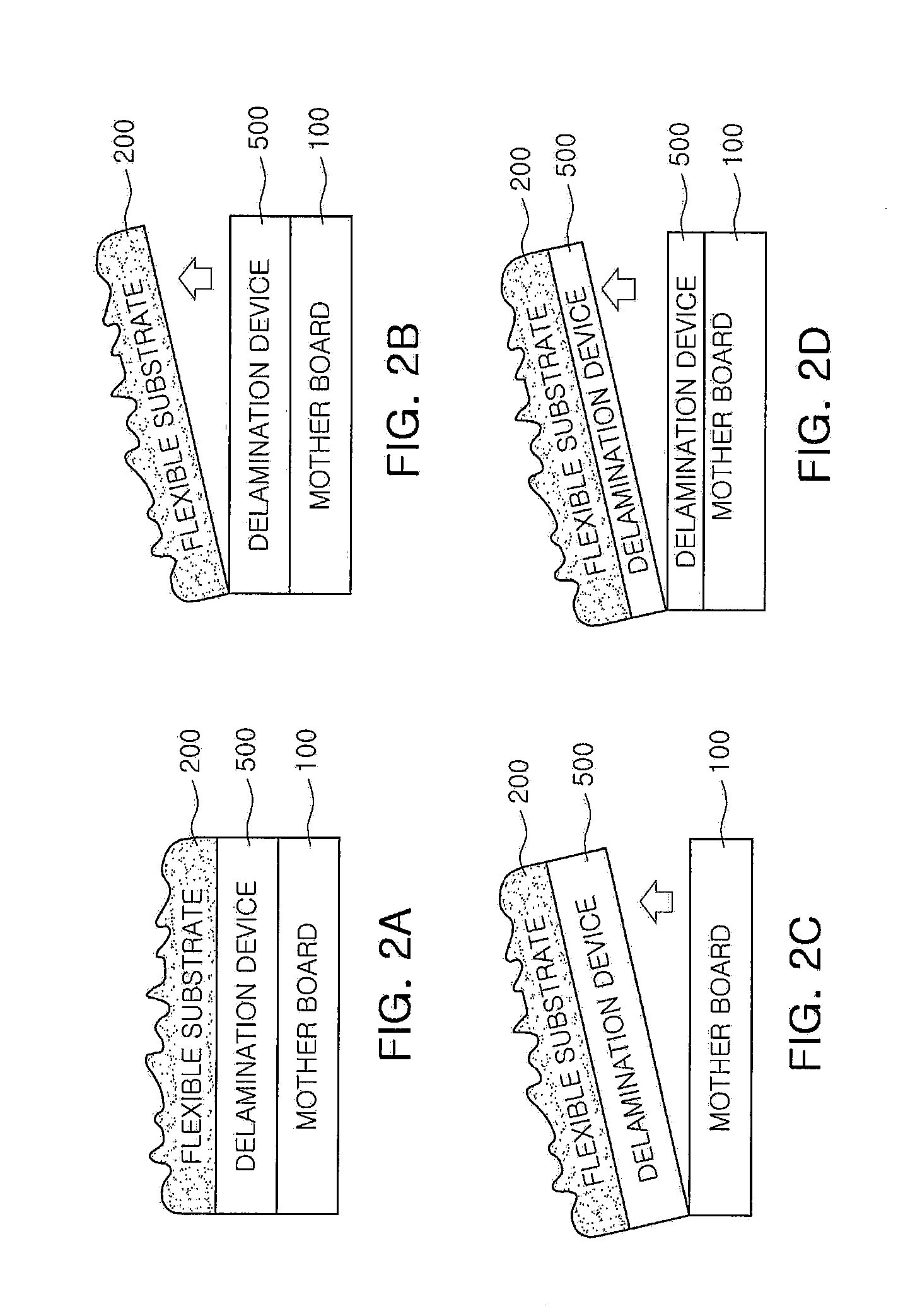
[0074]As illustrated in FIG. 2A, unlike Example 1, in Example 2, a flexible substrate 200 was manufactured through a method of forming a delamination layer 500 between a motherboard 100 and the flexible substrate 200. When the delamination layer 500 is formed thus, the flexible substrate 200 may be separated from an interface of the flexible substrate 200 (FIG. 2B), from an interface between the motherboard 100 and the delamination layer 500 (FIG. 2B), or from an inner surface of the delamination layer 500 (FIG. 2D). At this time, the case of FIG. 2B does not need a subsequent process, but the cases of FIGS. 2C and 2D may further include removing the delamination layer 500.

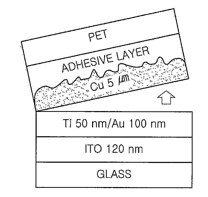
[0075]In Example 2 of the present invention, an ITO layer was formed as the delamination layer to a thickness of 120 nm on a glass substrate, a flexible substrate having a Ti / Au / Cu multilayered structure was formed on the ITO layer by respectively forming a Ti underlayer for the formation of a Cu layer and an Au s...

example 3

[0076]FIG. 3 schematically illustrates a method of manufacturing a flexible electronic device according to a third embodiment of the present invention. As illustrated in FIG. 3, in a method of manufacturing a flexible electronic device according to a third embodiment of the present invention, a flexible substrate 200 was formed on a motherboard 100 with a delamination layer 500 interposed therebetween (FIG. 3A), and an arbitrary substrate 600 was adhered on the flexible substrate 200 with an adhesive layer 700 interposed therebetween (FIG. 3C). Thereafter, the motherboard 100 formed on the flexible substrate 200 was separated using the delamination layer 500 (FIG. 3D), and an electronic device 300 and a sealant layer 400 were formed on a separated surface of the flexible substrate 200 to manufacture a flexible electronic device (FIG. 3E).

[0077]That is, the method in the third embodiment is different from that in the first embodiment in that it uses the arbitrary substrate 600 for ha...


PUM

PropertyMeasurementUnit
surface roughnessaaaaaaaaaa
thickaaaaaaaaaa
temperatureaaaaaaaaaa

Abstract

The present invention relates to resolving issues concerning deterioration in the performance and yield of a flexible electronic device, caused by low manufacturing temperatures, high degrees of surface roughness, a high thermal expansion coefficients, and bad handling characteristics of typical flexible substrates. The method for manufacturing a flexible electronic device according to the present invention includes: forming a flexible substrate on a motherboard while physically separating the interface therebetween so that the interfacial bonding therebetween has a yield strength less than that of the flexible substrate; and forming an electronic device on the separated surface of the flexible substrate which had previously been in contact with the motherboard.

Description

TECHNICAL FIELD[0001]The present invention relates to a flexible electronic device and a manufacturing method thereof, and a flexible substrate used in the flexible electronic device, and more particularly, to a method of manufacturing a flexible electronic device including a flexible substrate having low surface roughness and a low heat expansion coefficient applicable to a high temperature glass substrate process, and having superior characteristic and a new structure.BACKGROUND ART[0002]Currently, with development of information technology (IT), the importance of flexible electronic devices has increased. Thus, it is necessary to manufacture an organic light emitting display (OLED), a liquid crystal display (LCD), an electrophoretic display (EPD), a plasma display panel (PDP), a thin-film transistor (TFT), a microprocessor, a random access memory (RAM), or the like, on a flexible substrate.[0003]Among the above-described devices, an active matrix OLED (AMOLED) has come to promine...

Claims


Application Information

Patent Timeline
Patent Type & Authority Applications(United States)
IPC IPC(8): H05K3/30H05K1/02
CPCH01L51/003H01L51/0097H01L51/52H01L51/56H01L2227/326H01L2251/5338Y10T29/4913H05K3/303Y02E10/549H01L29/78603H01L27/1218H01L27/1266H05K1/0277Y02P70/50H10K71/80H10K77/111H10K50/80H10K59/1201H10K71/00H10K2102/311
Inventor LEE, JONG LAMKIM, KEE SOO
Owner POHANG IRON & STEEL CO LTD
Why Eureka
Try Eureka