Interconnect structure and sputtering target

a thin film transistor and interconnect structure technology, applied in the direction of electrolysis components, vacuum evaporation coatings, coatings, etc., can solve the above-described deterioration of tft characteristics by stress, lowering of reliability in the display device itself, etc., to achieve excellent switching characteristics, small variation, and high stress resistance

Active Publication Date: 2013-09-26
KOBE STEEL LTD
View PDF5 Cites 36 Cited by
  • Summary
  • Abstract
  • Description
  • Claims
  • Application Information

AI Technical Summary

Benefits of technology

[0021]The interconnect structure of the present invention has excellent switching characteristics and high stress resistance, and in particular, shows a small variation of threshold voltage before and after the stress tests, and therefore, interconnect structures were able to

Problems solved by technology

In addition, for example, when a liquid crystal panel is driven or when a negative bias is applied to the gate electrode to turn on a pixel, the TFT is irradiated with light leaked out from the liquid crystal cell, and this light gives stress to the TFT to cause a deterioration in the characteristics.
Indeed, when a thin-film transistor is used, a variation of switching characteristics due to stress by voltage application causes a lowering of reliability in a display devices itself, such as a liquid crystal display or an organic EL display.
The above-described deterioration in the TFT characteristics by stress such as voltage application or light irradiation is due to the formation of defects in the semiconductor itself or

Method used


Image

  • Interconnect structure and sputtering target
  • Interconnect structure and sputtering target
  • Interconnect structure and sputtering target

Examples


examples

[0078]The present invention will hereinafter be described more specifically by way of Examples, but the present invention is not limited to the following Examples. The present invention can be put into practice after appropriate modifications or variations within a range meeting the gist described above and below, all of which are included in the technical scope of the present invention.

experiment 1

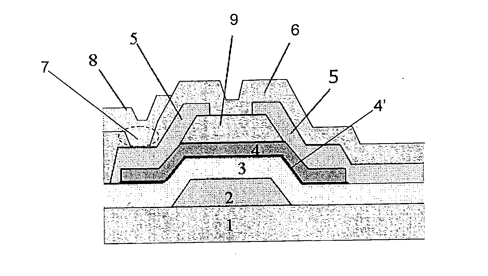
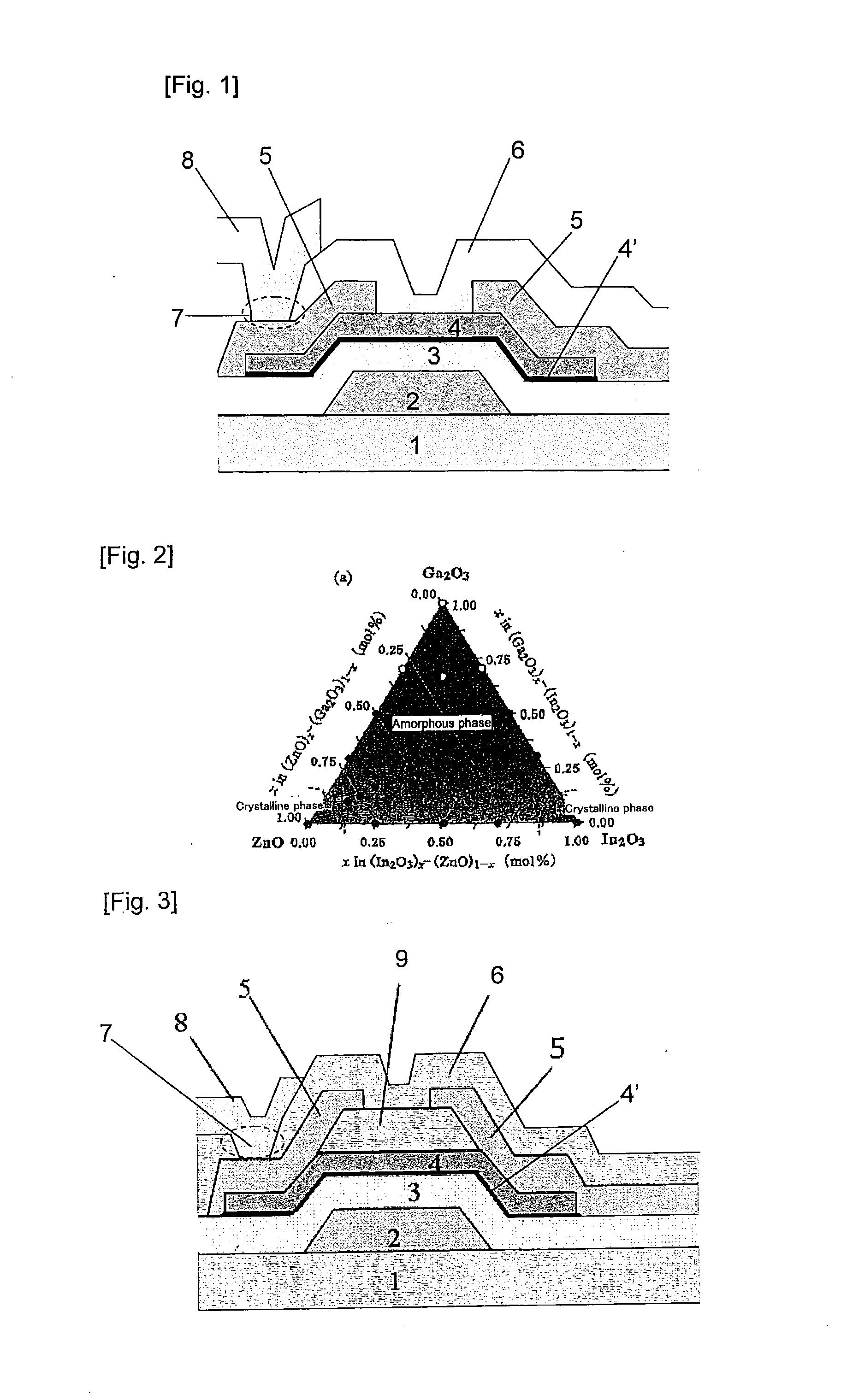
[0079]According to a method as described above, a thin-film transistor (TFT) shown in FIG. 1 was produced, and TFT characteristics before and after the formation of a passivation layer (insulator layer) 6 were evaluated (in this experiment, an etch stopper layer 9 was not formed).

[0080]First, a Ti thin-film of 100 nm in thickness as a gate electrode 2 and SiO2 (200 nm) as a gate insulator layer 3 were successively formed on a glass substrate 1 (“EAGLE 2000” available from Corning Incorporated, having a diameter 100 mm and a thickness of 0.7 mm). The gate electrode 2 was formed using a pure Ti sputtering target by a DC sputtering method under the conditions: film formation temperature, room temperature; film formation power, 300 W; carrier gas, Ar; and gas pressure, 2 mTorr. Further, the gate insulator layer 3 was formed by a plasma CVD method under the conditions: carrier gas, a mixed gas of SiH4 and N2O; film formation power, 100 W; and film formation temperature, 300° C.

[0081]Then...

experiment 2

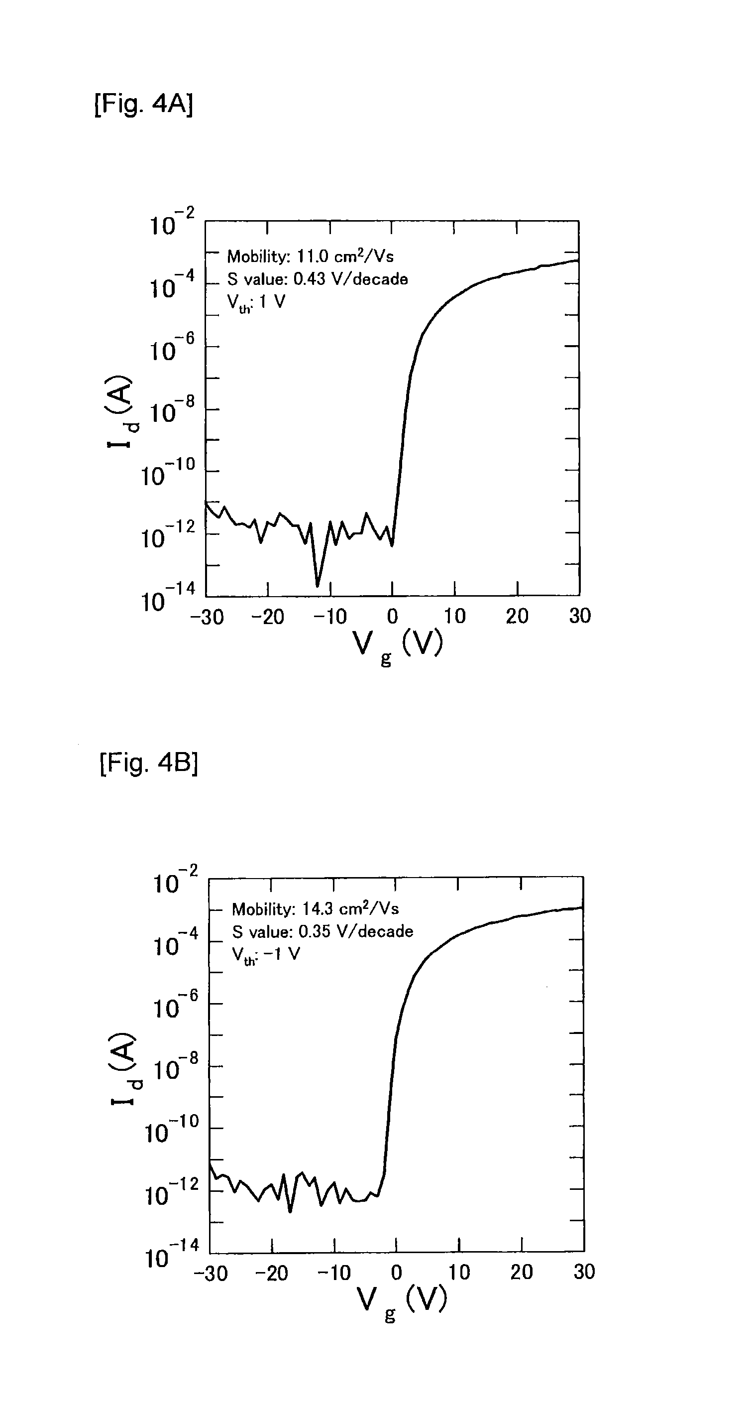
[0124]Various TFTs were produced in the same manner as Experiment 1 described above, except that the kind of the Y group element contained in the second oxide semiconductor layer in the oxide semiconductor layer (a layered product formed by the first oxide semiconductor layer (IGZO) and the second oxide semiconductor layer (IGZO+the Y group element)) of the present invention was changed. The composition of IGZO (the Z group element and the X group element) in the first oxide semiconductor layer and the second oxide semiconductor layer was set to be In:Ga:Zn=2:2:1. The first oxide semiconductor layer was set to have a thickness of 50 nm and the second oxide semiconductor layer was set to have a thickness of 5 nm, and both layers were formed in a continuous manner using a DC sputtering method. The TFTs were measured for TFT characteristics and subjected to the stress test. The results are shown in Table 1.

[0125]In Table 1, the threshold voltage variation Δth=−6.2 V (1 hour) in the str...


PUM

PropertyMeasurementUnit
Thicknessaaaaaaaaaa
Thicknessaaaaaaaaaa
Densityaaaaaaaaaa

Abstract

The interconnect structure of the present invention includes at least a gate insulator layer and an oxide semiconductor layer on a substrate, wherein the oxide semiconductor layer is a layered product having a first oxide semiconductor layer containing at least one element (Z group element) selected from the group consisting of In, Ga, Zn and Sn; and a second oxide semiconductor layer containing at least one element (X group element) selected from the group consisting of In, Ga, Zn and Sn and at least one element (Y group element) selected from the group consisting of Al, Si, Ti, Hf, Ta, Ge, W and Ni, and wherein the second oxide semiconductor layer is interposed between the first oxide semiconductor layer and the gate insulator layer. The present invention makes it possible to obtain an interconnect structure having excellent switching characteristics and high stress resistance, and in particular, showing a small variation of threshold voltage before and after the stress tests, and thereby having high stability.

Description

TECHNICAL FIELD[0001]The present invention relates to an interconnect structure of thin-film transistors (TFTs) to be used in display devices such as liquid crystal displays and organic EL displays; and a sputtering target.BACKGROUND ART[0002]As compared with widely used amorphous silicon (a-Si), amorphous (non-crystalline) oxide semiconductors have high carrier mobility (also called as field-effect mobility, which may hereinafter be referred to simply as “mobility”), high optical band gaps, and film formability at low temperatures, and therefore, have highly been expected to be applied for next generation displays, which are required to have large sizes, high resolution, and high-speed drives; resin substrates having low heat resistance; and others.[0003]In the oxide semiconductors, amorphous oxide semiconductors consisting of indium, gallium, zinc and oxygen (In—Ga—Zn—O, which may hereinafter be referred to as “IGZO”) have preferably been used, in particular, because of their havi...

Claims


Application Information

Patent Timeline
IPC IPC(8): H01L29/786C23C14/14
CPCC23C14/086H01L21/02554H01L21/02565H01L21/02581H01L21/02614H01L29/78693H01L29/7869H01L21/02573C23C14/14C23C14/34H01L21/02631
Inventor MORITA, SHINYAMIKI, AYAYASUNO, SATOSHIKUGIMIYA, TOSHIHIRO
Owner KOBE STEEL LTD
Why Eureka
Try Eureka