Illumination device

a technology of a spherical device and a spherical tube, which is applied in the direction of semiconductor devices for light sources, lighting and heating apparatus, instruments, etc., can solve the problems of high local heat dissipation, emission directionality problems, and difficulty in limiting usefulness, so as to enhance the excitation of the wavelength conversion medium, improve the wavelength conversion process, and improve the coupling of the primary

Active Publication Date: 2013-10-31
LUMILEDS
View PDF4 Cites 41 Cited by
  • Summary
  • Abstract
  • Description
  • Claims
  • Application Information

AI Technical Summary

Benefits of technology

[0013]An embodiment of the invention according to claim 2 provides the advantage of improving the wavelength conversion process through the coupling of the incident primary wavelength light or the emitted secondary light to the surface lattice resonances that arise from the diffractive coupling of localized surface plasmon polaritons in the individual antennas of the array.
[0014]According to an embodiment of the invention, the periodicity of the antenna array is of the order of the primary or secondary wavelength light. Beneficially, this allows the light to excite surface lattice resonances.
[0015]The embodiment of the illumination device according to claim 4 beneficially allows controlling the modification of the illumination distribution of the device. This modification of the emitted light distribution from Lambertian to a more confined solid angle is especially interesting for low etendue lighting applications such as projection in beamers and automotive front lighting.
[0016]The embodiment of the invention of claim 5 advantageously allows for a better coupling of the primary and / or secondary wavelength light with the antennas and surface lattice resonances of the array.
[0017]In an embodiment according to claim 6, the stretchably controllable substrate allows active control of the emission efficiency, the directionality of the emission, and the emitted wavelength of the illumination device.
[0018]In embodiments according to claims 7 to 10, the two sub-arrays allow for appropriately designing the antenna array to accommodate several optical phenomena, such as, for instance, one sub-array enhances the excitation of the wavelength conversion medium, while the other sub-array enhances the emission of and defines the direction of the secondary wavelength light.

Problems solved by technology

Devices as disclosed by U.S. Pat. No. 7,709,811 exhibit several difficulties limiting their usefulness, such as heat management issues, efficiency issues, and emission directionality issues.
When concentrating light with such power levels in a relative small volume of phosphor material, the Stokes losses inherent to the wavelength conversion process result in high local heat dissipation.
This results in alleviated temperature levels of the phosphor which can easily exceed 200-300° C. At such levels, the conversion efficiency of the phosphors drops significantly, potentially resulting in additional power losses and uncontrolled further heating.
Such relatively large thicknesses may lead to an extended size of the light emitting area, especially when used in combination with laser light sources, and thus to a limited use of such devices as low éndue light sources in f.i. projection applications as beamers or car head lights.
While beam shaping optical elements are known to be useful to realize the application specific illumination distribution, these optical elements are usually bulky, need precise alignment with the LED and / or wavelength converting material, and are typically based on weakly dispersing materials (e.g. glass, plastics) which do not allow different beam shaping and beam directing of different light colors.

Method used


Image

  • Illumination device
  • Illumination device
  • Illumination device

Examples


Embodiment Construction

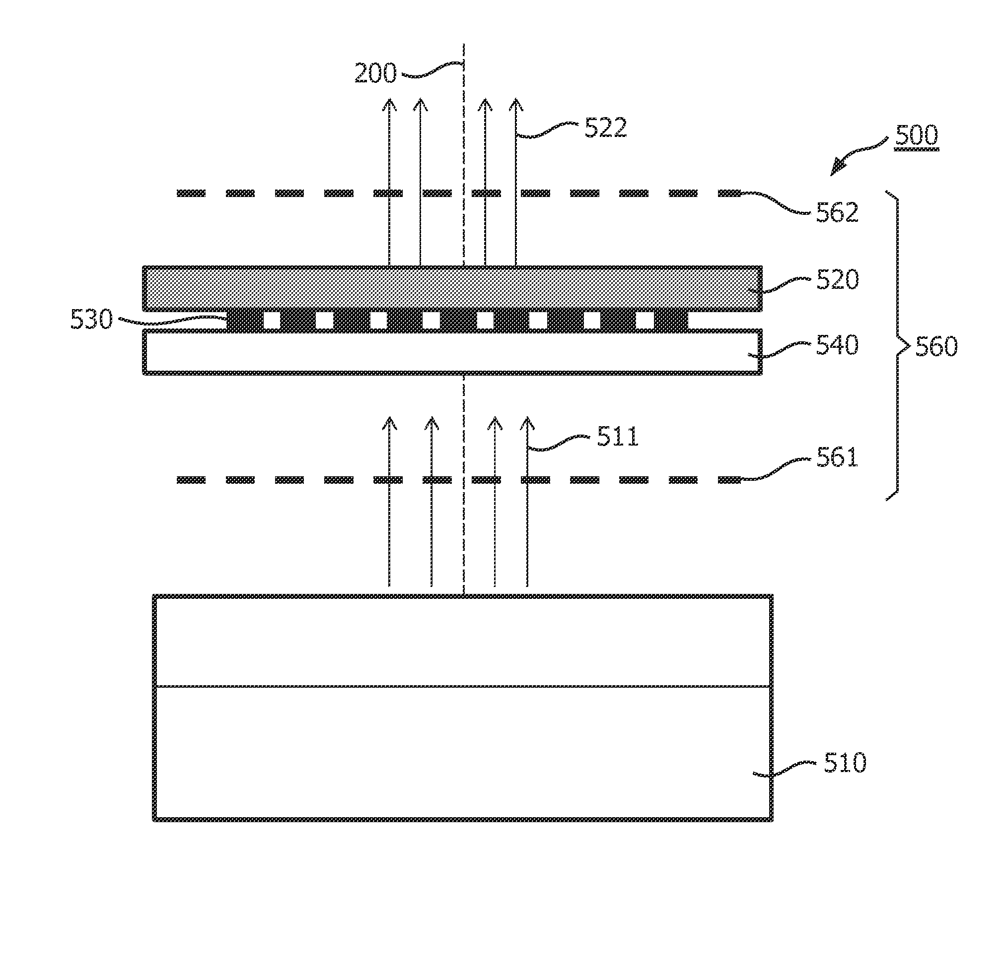
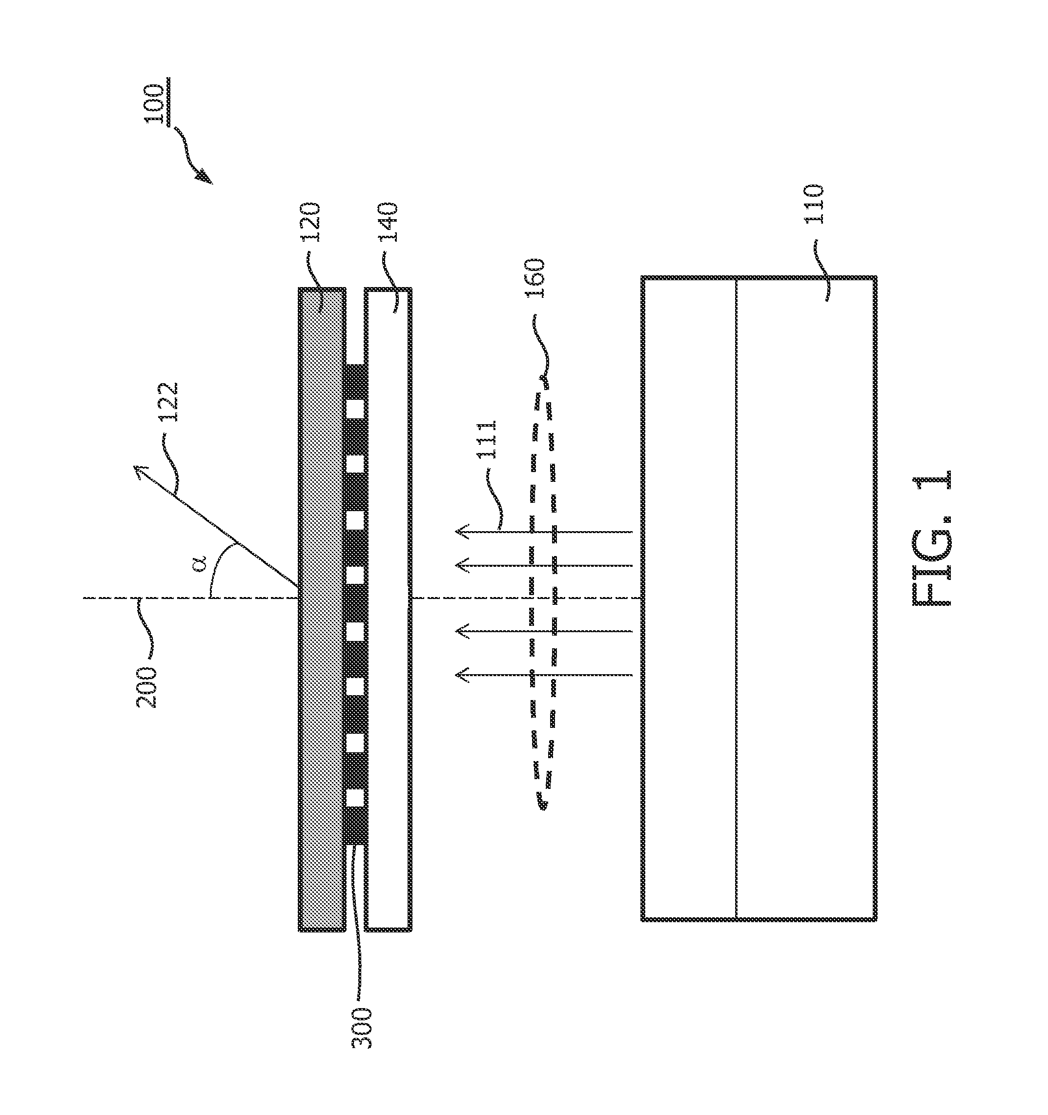
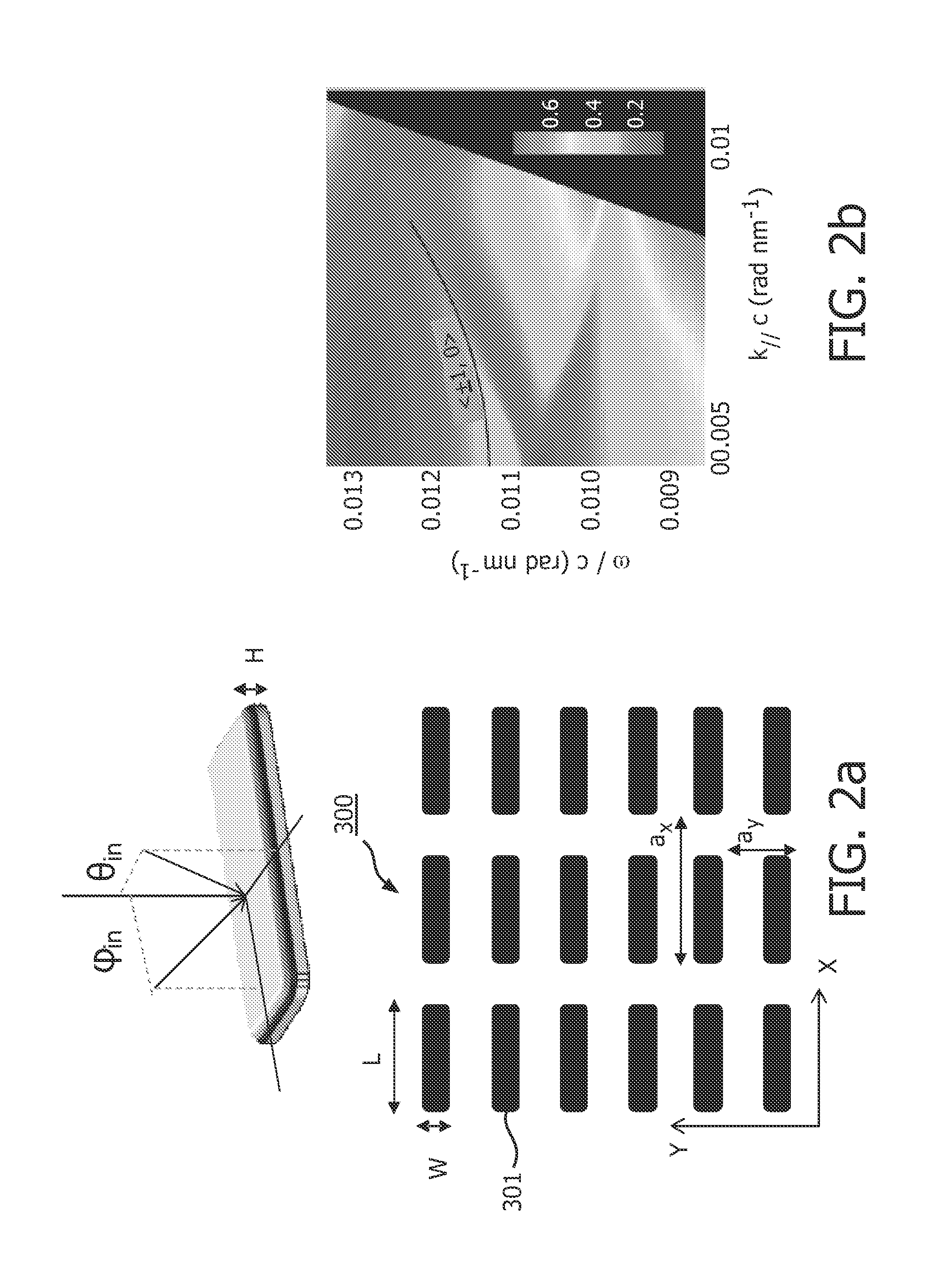
[0032]FIG. 1 shows an illumination device 100 in accordance with the invention. The illumination device 100 comprises a light source 110, for instance a semiconductor light source such as a (inorganic or organic) light emitting diode (LED), a resonant cavity light emitting diode, a laser diode (LD), such as a vertical cavity laser diode or an edge emitting laser diode. Material systems currently of interest in the manufacture of such semiconductor light sources capable of operating in the visible spectrum include Group III-V semiconductors. In particular binary, ternary, and quaternary alloys of gallium, aluminium, indium, and nitrogen, also referred to as III-nitride materials, are of interest. Typically, III-nitride semiconductor light sources are fabricated by epitaxially growing a stack of semiconductor layers of different composition and dopant concentrations on a sapphire, silicon carbide, III-nitride, or other suitable substrate by metal-organic chemical vapour deposition, mo...


PUM


Abstract

Proposed is an illumination device (100), comprising a light source (110) such as an LED or a laser diode, a wavelength conversion medium (120) such as a phosphor, and a periodic antenna array (300) made of a highly polarisable material such as a metal. The light source emits primary wavelength light that at least partially is converted in secondary wavelength light by the wavelength conversion medium. The periodic antenna array is positioned in close proximity to the wavelength conversion medium and functions to enhance the efficiency of the absorption and/or emission processes in the wavelength conversion medium through the coupling of the incident primary wavelength light or the emitted secondary light to surface lattice resonances that arise from the diffractive coupling of localized surface plasmon polaritons in the individual antennas of the array. This is especially advantageous for forming low étendue illumination device suitable for use in projection systems, or for controlling the directionality, the polarization, and/or the color of the secondary wavelength light.

Description

FIELD OF THE INVENTION[0001]The invention relates to an illumination device. In particular it relates to such a device applying a wavelength conversion medium. Such a device is used in, for example, illumination systems, projection systems, and laser systems.BACKGROUND OF THE INVENTION[0002]An embodiment of an illumination device of the kind set forth is known from U.S. Pat. No. 7,709,811. That document discloses an illumination device comprising a blue LED (e.g. GaN or InGaN) light source, an internal optical element, a wavelength converting material, and an external optical element (e.g. a plastic or glass lens). The wavelength converting material (e.g. an organic dye or inorganic phosphor) is applied to a side of the internal element facing away from the LED. The internal optical element is a rectangular or pyramid shaped prism and serves to direct primary light emitted by the LED to the wavelength converting material. Moreover, it serves to redirect secondary light emitted by th...

Claims


Application Information

Patent Timeline
Patent Type & Authority Applications(United States)
IPC IPC(8): F21V9/08
CPCF21V9/08H01L33/50H01L33/58G03B21/204F21Y2115/30F21K9/64C09K11/56C09K11/7774C09K11/883F21Y2115/10C09K11/0883C09K11/676C09K11/7769F21V13/08F21V9/32F21V9/38G02B5/18F21K9/62G02B5/008H01L33/502
Inventor RODRIGUEZ, SAID RAHIMZADEH KALALEHRIVAS, JAIME GOMEZBALKENENDE, ABRAHAM RUDOLFVERSCHUUREN, MARCUS ANTONIUSLOZANO BARBERO, GABRIEL SEBASTIANMURAI, SHUNSUKE
Owner LUMILEDS
Why Eureka
Try Eureka