SiOx n-LAYER FOR MICROCRYSTALLINE PIN JUNCTION

a microcrystalline pin and n-layer technology, applied in the direction of photovoltaic energy generation, basic electric elements, electrical apparatus, etc., can solve the problems of low deposition rate, long deposition time, loss of light in the cell, etc., to reduce production time and cost, simplify the structure, and simplify production

Inactive Publication Date: 2013-11-07
OERLIKON SOLAR AG (TRUEBBACH)
View PDF4 Cites 3 Cited by
  • Summary
  • Abstract
  • Description
  • Claims
  • Application Information

AI Technical Summary

Benefits of technology

[0022]Upon this front electrode is provided directly or indirectly at least one p-i-n junction of at least one photovoltaic light conversion layer stack. Each stack comprises a p-doped silicon layer, and essentially intrinsic silicon layer provided directly or indirectly upon the p-doped silicon layer, and an n-doped layer provided directly or indirectly on the intrinsic silicon layer. A back electrode is finally provided on the n-doped layer. The back electrode is provided directly on the n-doped layer situated furthest from the substrate, which in the case of a single layer stack would be the only n-doped layer, and this n-doped layer consists of a silicon- and oxygen-containing doped microcrystalline layer, that is to say that the layer is deposited under a process regime suitable for depositing a microcrystalline layer. This eliminates the requirement for any intermediate adhesion or interface layers, thus simplifying production and reducing production time and costs.
[0023]In an embodiment, the n-doped layer is provided directly on the essentially intrinsic silicon layer. This simplifies the structure and reduces production time and costs. In addition, arranging the SiOx n-doped layer directly on the intrinsic layer has a backside passivation effect on the intrinsic silicon layer, reducing the problems created by a highly uneven interface surface, and increasing the efficiency and longevity of the light conversion device.
[0024]In an embodiment, the oxygen content of the n-doped layer is chosen such that the refractive index n of the n-doped layer at a wavelength of light of 500 nm is greater than or equal to 2.0. This enables the n-doped layer additionally to function as a reflector, thus increasing the efficiency of the light conversion device by causing more light to be reflected back into the absorber layer before reaching the back electrode, since this reflected light does not have to...

Problems solved by technology

However, due to its low band gap of 1.1 eV highly crystalline microcrystalline silicon exhibits a high absorption in the long wavelength part of the spectra, thus leading to a loss of light in the cell.
In addition, highly crystalline microcrystalline silicon is usually prepared in a deposition regime using a very high hydrogen dilution ratio of the process gases, leading to a low deposition rate and therefore, long deposition time, which is detrimental to the throughput of a production system and therefore, for production cost.
However, amorphous silicon has a far lower doping effici...

Method used


Image

  • SiOx n-LAYER FOR MICROCRYSTALLINE PIN JUNCTION
  • SiOx n-LAYER FOR MICROCRYSTALLINE PIN JUNCTION

Examples


Embodiment Construction

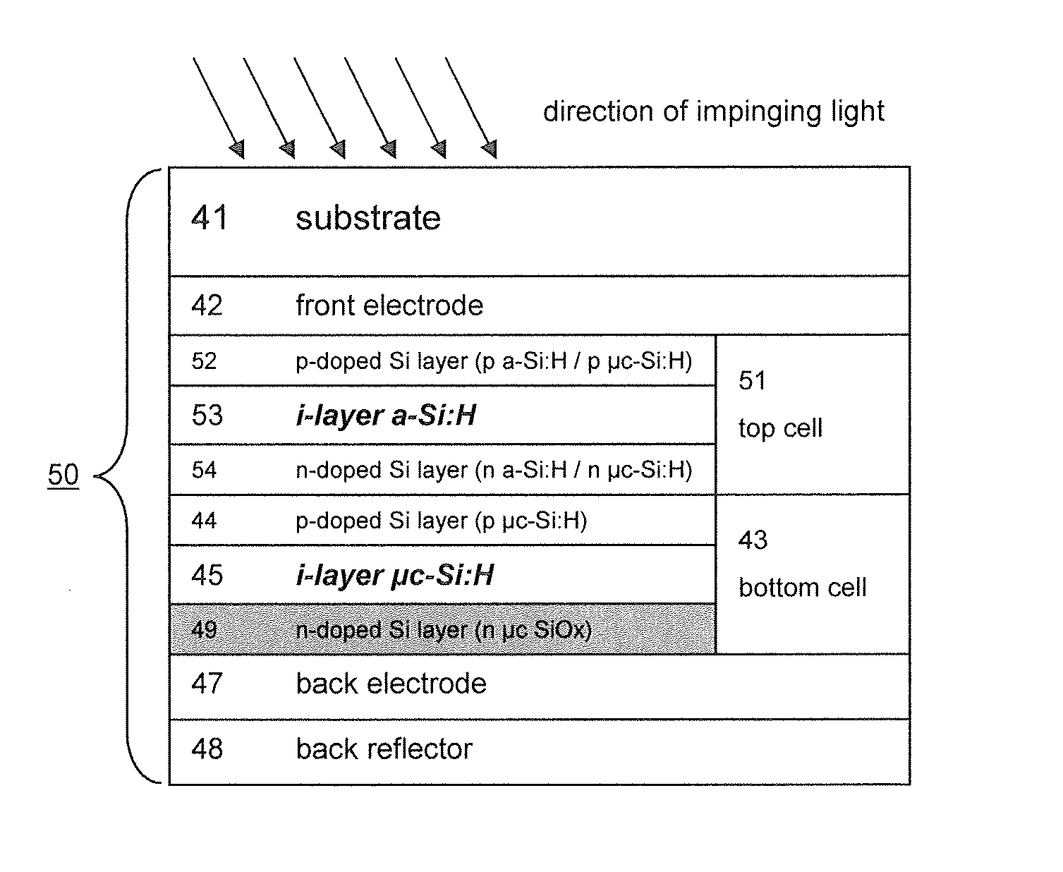
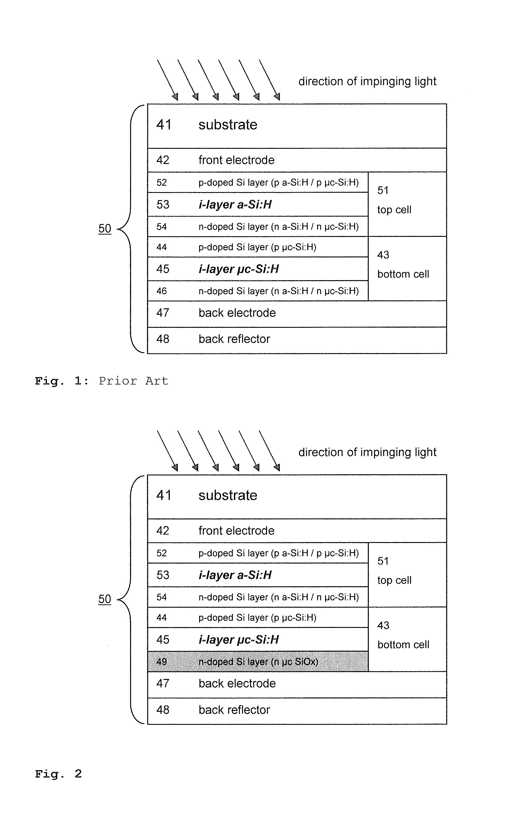
[0030]It was found that both requirements for the n-layer such as high transmission in the long wavelength part of the spectra as well as a contribution to back reflection of light into the absorber layer before reaching the back contact in combination with sufficiently good electrical behavior can be achieved even without a second contact layer. It could be shown that it is possible to obtain this by applying a single SiOx n-type layer 49 (FIG. 2) in place of the conventional n-doped silicon layer 46 of prior art (FIG. 1), when the properties of such a layer are optimized in an appropriate range in combination with an appropriate n-layer / back contact interface. The optimization can be realized by[0031]a) Choosing the oxygen content of such an inventive SiOx layer in a range that the refractive index n at a wavelength of the light of 500 nm is in not smaller than 2.0.[0032]b) Increasing the doping of said inventive SiOx layer by a sufficiently high dopant gas flow to achieve a reaso...


PUM


Abstract

The present invention concerns a light conversion device comprising at least direction of impinging light one photovoltaic light conversion layer stack (43, 51) comprising a p-i-n junction and situated between a front (42) and back (47) electrode, wherein the n-layer (49) of the layer stack (43) situated closest to the back electrode (47) consists of a n-doped silicon- and oxygen-containing (SiOx) microcrystalline layer, and is in direct contact with the back electrode (47). The invention equally concerns a corresponding method for manufacturing such a light conversion device. The requirement for intermediate adhesion/interface layers between SiOx layer and back electrode can thus be obviated, resulting in simplified manufacture.

Description

FIELD OF THE INVENTION[0001]Photovoltaic solar energy conversion offers the perspective to provide for an environmentally friendly means to generate electricity. Therefore, the development of more cost-effective means of producing photovoltaic energy conversion units attracted attention in the recent years. Amongst different approaches for producing low-cost solar cells, thin film silicon solar cells combine several advantageous aspects: firstly, thin-film silicon solar cells can be prepared by known thin-film deposition techniques such as plasma enhanced chemical vapor deposition (PECVD) and thus offer the perspective of synergies to reduce manufacturing cost by using experiences from display production technology. Secondly, thin-film silicon solar cells can achieve high energy conversion efficiencies striving towards 10% and beyond. Thirdly, the main raw materials for the production of thin-film silicon based solar cells are abundant and non-toxic.DEFINITIONS[0002]Processing in th...

Claims


Application Information

Patent Timeline
IPC IPC(8): H01L31/076H01L31/18
CPCH01L31/076H01L31/182H01L31/02167H01L31/075Y02E10/546Y02E10/548
Inventor KUPICH, MARKUSLEPORI, DANIEL
Owner OERLIKON SOLAR AG (TRUEBBACH)
Why Eureka
Try Eureka