Method of making cavity substrate with built-in stiffener and cavity

Inactive Publication Date: 2013-12-19
BRIDGE SEMICON
View PDF2 Cites 46 Cited by
  • Summary
  • Abstract
  • Description
  • Claims
  • Application Information

AI Technical Summary

Benefits of technology

[0045]The present invention has numerous advantages. The stiffener provides a mechanical support for the coreless build-up circuitry or the interconnect substrate. The metal block formed by removing a selected portion of the sacrificial carrier can only be separated from the dielectric layer by etching to create a cavity area for device placement and thus ensure a high manufacturing yield without un-predictable peeling or delamination concern. Furthermore, vast options of the built-in stiffener ranging from low coefficient of thermal expansion (CTE) materials like ceramics, to high thermal conductive materials like metal plate, to low cost materials like glass-fiber epoxy provide diversified solutions for various packaging designs. As a re

Problems solved by technology

As plated-through-hole in the copper-clad laminate core is typically formed by mechanical CNC drill, reducing its diameter in order to increase wiring density may encounter seriously technical limitations and often very costly.
However, as coreless boards do not have a core layer to provide a necessary flexural rigidity, they are more susceptible to warpage problem when under thermal stress compared to that of conventional boards with core layers.
In this approach, although a supporting platform can be created a

Method used


Image

  • Method of making cavity substrate with built-in stiffener and cavity
  • Method of making cavity substrate with built-in stiffener and cavity
  • Method of making cavity substrate with built-in stiffener and cavity

Examples


embodiment 1

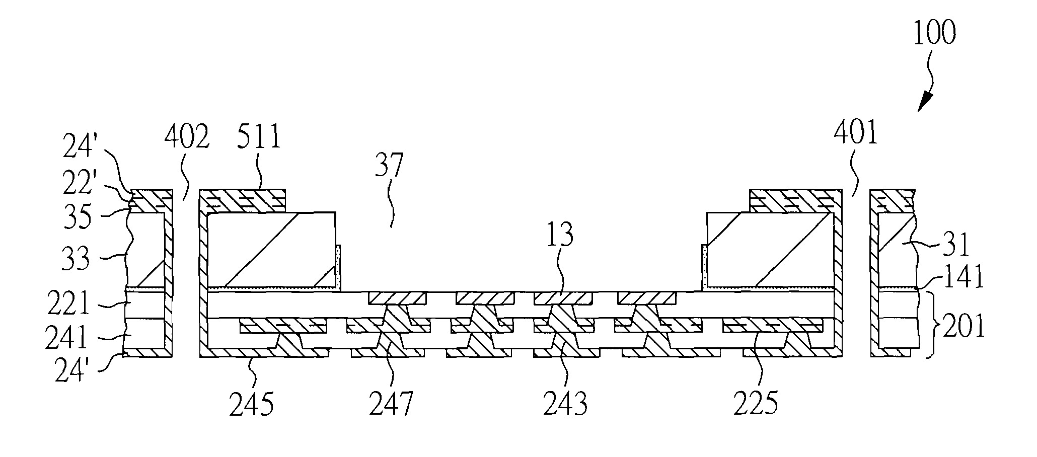
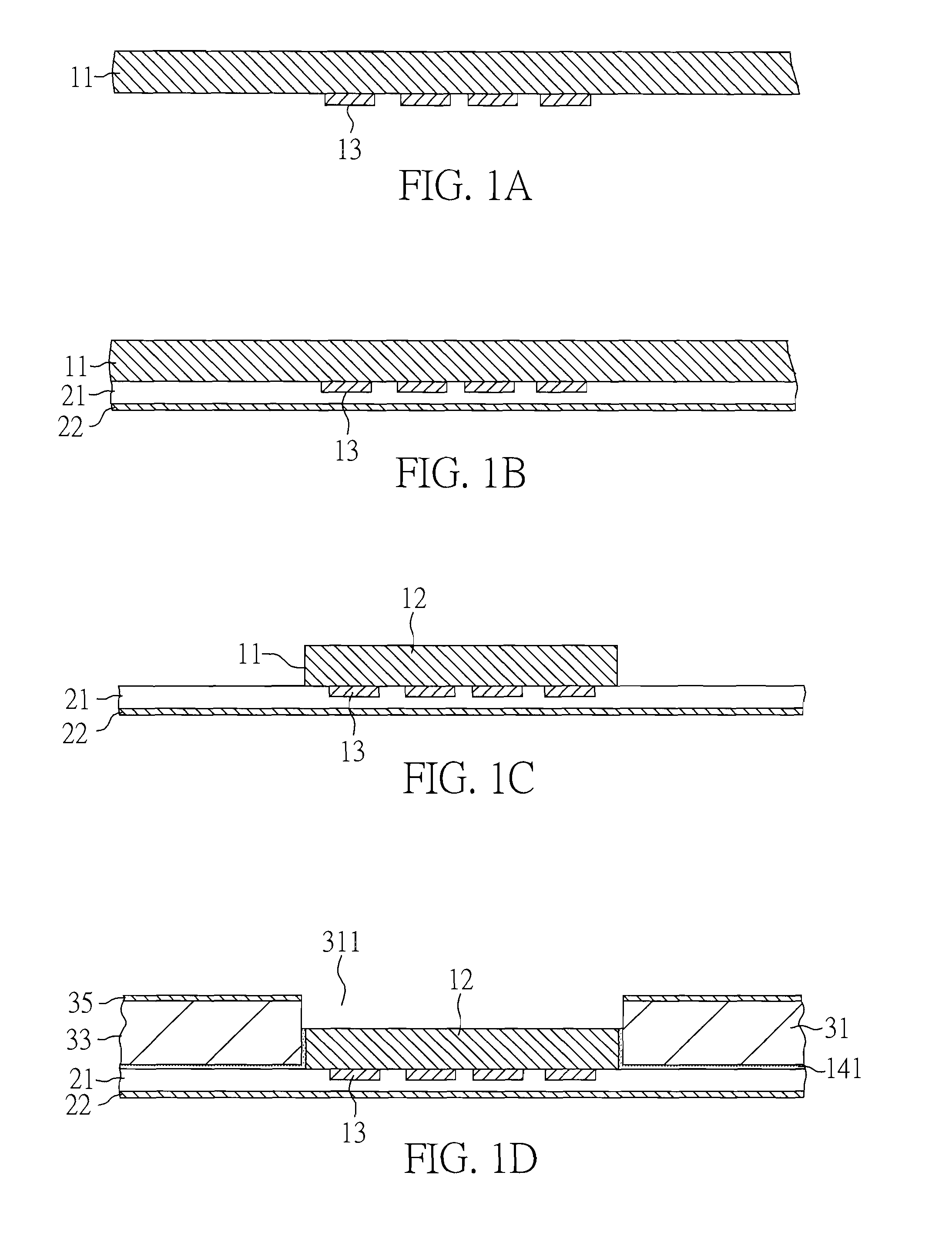
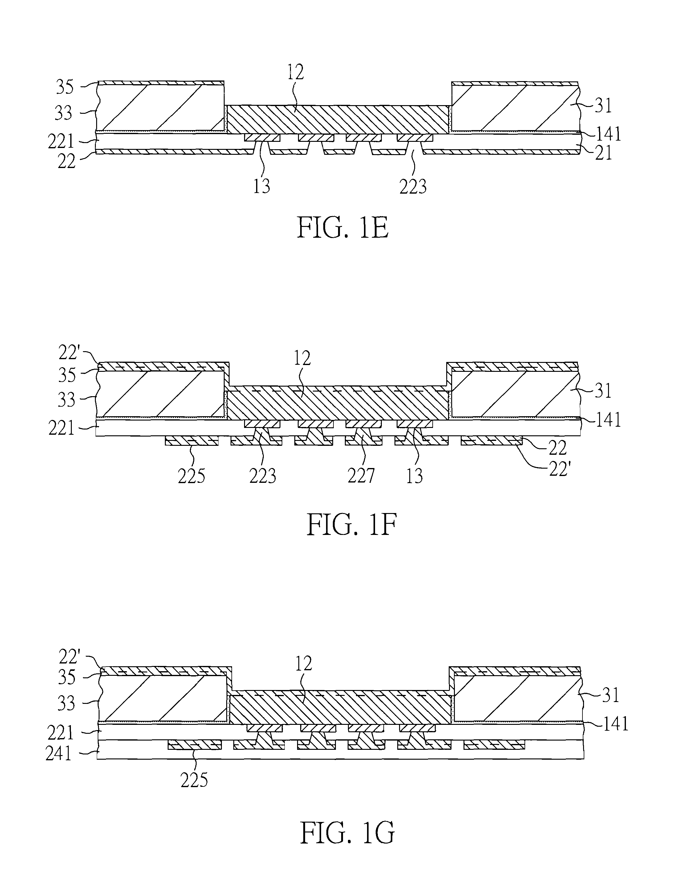
[0055]FIGS. 1A-1J are cross-sectional views showing a method of making a cavity substrate that includes electrical pads exposed from a cavity, a stiffener, an adhesive, a build-up circuitry in electrical connection with the electrical pads, terminals and plated through-holes that provide an electrical connection between the build-up circuitry and the terminals in accordance with one embodiment of the present invention.

[0056]FIG. 1A is a cross-sectional view of the structure with electrical pads 13 on sacrificial carrier 11. Sacrificial carrier 11 typically is made of copper, but other materials such as aluminum, alloy 42, iron, nickel, silver, gold, tin, combinations thereof, and alloys thereof are also doable. In consideration of process and cost, the thickness of sacrificial carrier 11 preferably ranges from 125 to 500 microns. Electrical pads 13 extend from sacrificial carrier 11 in the downward direction and are covered by sacrificial carrier 11 in the upward direction. Electric...

embodiment 2

[0079]FIGS. 2A-2G are cross-sectional views showing a method of making a cavity substrate that includes a stiffener, an adhesive, a build-up circuitry that includes conductive vias exposed from a cavity, terminals and plated through-holes that provide an electrical connection between the build-up circuitry and the terminals in accordance with another embodiment of the present invention.

[0080]For purposes of brevity, any description in above Embodiment is incorporated herein insofar as the same is applicable, and the same description need not be repeated.

[0081]FIG. 2A is a cross-sectional view of the structure with sacrificial carrier 11 laminated with metal layer 22 using dielectric layer 21 between sacrificial carrier 11 and metal layer 22. Sacrificial carrier 11 can be various metals such as copper, aluminum, alloy 42, iron, nickel, silver, gold, tin, combinations thereof, and alloys thereof. In order to prevent conductive vias subsequently formed in contact with sacrificial carri...

embodiment 3

[0090]FIGS. 3A-3H are cross-sectional views showing a method of making a cavity substrate that includes a stiffener, an adhesive, a dielectric layer, an interconnect substrate, conductive vias electrically connected to the interconnect substrate and exposed from a cavity, terminals and a plated through-hole that provides an electrical connection between the interconnect substrate and the terminals in accordance with yet another embodiment of the present invention.

[0091]For purposes of brevity, any description in above Embodiments is incorporated herein insofar as the same is applicable, and the same description need not be repeated.

[0092]FIG. 3A is a cross-sectional view of the structure with sacrificial carrier 11 laminated onto interconnect substrate 202 using dielectric layer 21, such as epoxy resin, glass-epoxy, polyimide and the like with a thickness of 50 microns. Interconnect substrate 202 includes first circuitry layer 214, first insulating layer 231, metal layer 25 and firs...


PUM


Abstract

The present invention relates to a method of making a cavity substrate. In accordance with a preferred embodiment, the method includes: providing a sacrificial carrier and optionally an electrical pad that extends from the sacrificial carrier in the first vertical direction; providing a dielectric layer that covers the sacrificial carrier in the first vertical direction; removing a selected portion of the sacrificial carrier; attaching a stiffener to the dielectric layer from the second vertical direction; forming a build-up circuitry from the first vertical direction; and removing the remaining portion of the sacrificial carrier to expose electrical contacts from the second vertical direction. A semiconductor device can be mounted on the cavity substrate and electrically connected to the electrical contacts within the built-in cavity of the cavity substrate. The stiffener can provide mechanical support for the build-up circuitry and the semiconductor device.

Description

CROSS REFERENCE TO RELATED APPLICATION[0001]This application claims the benefit of filing date of U.S. Provisional Application Ser. No. 61 / 659,491, entitled “Cavity Substrate with Electrical Contacts Exposed from Cavity and Stackable Semiconductor Assembly Using the Same and Method of Making the Same” filed Jun. 14, 2012 under 35 USC §119(e)(1).BACKGROUND OF THE INVENTION[0002]1. Field of the Invention[0003]The present invention relates to a method of making a cavity substrate, and more particularly to a method of making a cavity substrate with one or more electrical contacts exposed from a built-in cavity.[0004]2. Description of Related Art[0005]Latest trends of electronic devices such as mobile internet devices (MIDs), multimedia devices and computer notebooks demand for faster and slimmer designs. In the frequency band of a general signal, the shorter paths of circuitry, the better the signal integrity. Thus, the size of inter-layer connection, i.e., the diameter of the micro-via...

Claims


Application Information

Patent Timeline
IPC IPC(8): H01L21/48
CPCH01L21/486H01L23/13H01L21/4857H01L23/5389H01L2924/351H01L2924/15787H01L2924/12042H01L2224/16227H01L2224/73204H01L2224/73253H01L2924/15153H01L2924/15311H01L2924/18161H01L2924/00
Inventor LIN, CHARLES W.C.WANG, CHIA-CHUNG
Owner BRIDGE SEMICON
Why Eureka
Try Eureka