

Light-emitting device and method for fabricating the same
- Summary
- Abstract
- Description
- Claims
- Application Information
AI Technical Summary
Benefits of technology
Problems solved by technology
Method used
Image

Examples
embodiment 1
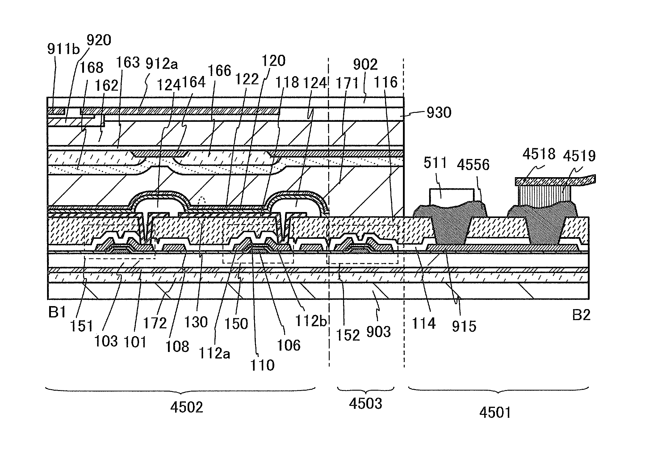
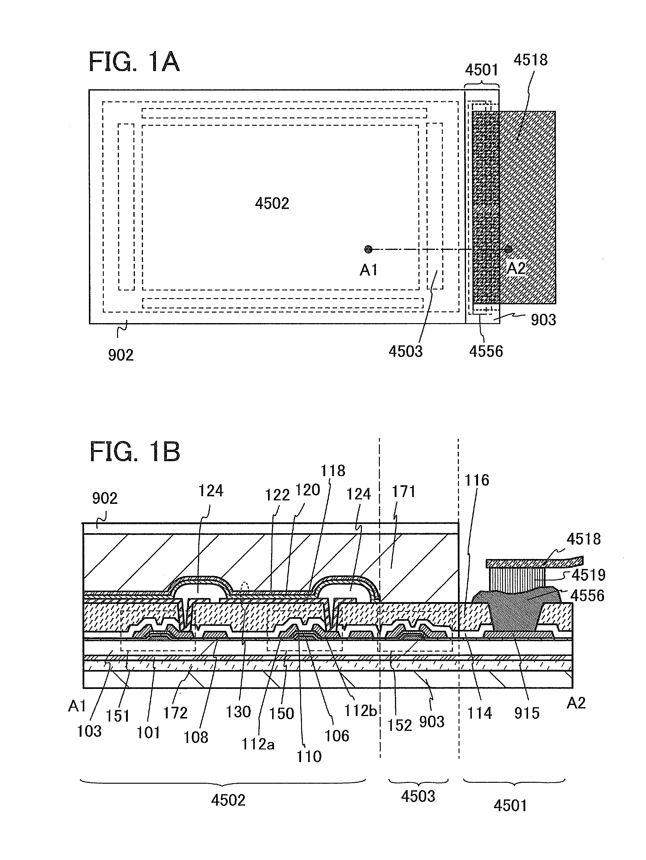
[0036]FIG. 1A is a top view of a light-emitting device according to one embodiment of the present invention, and FIG. 1B is a cross-sectional view taken along the line A1-A2 in FIG. 1A.
[0037]A light-emitting device illustrated in FIG. 1A includes a terminal portion 4501, a pixel portion 4502, and a signal line circuit portion 4503.
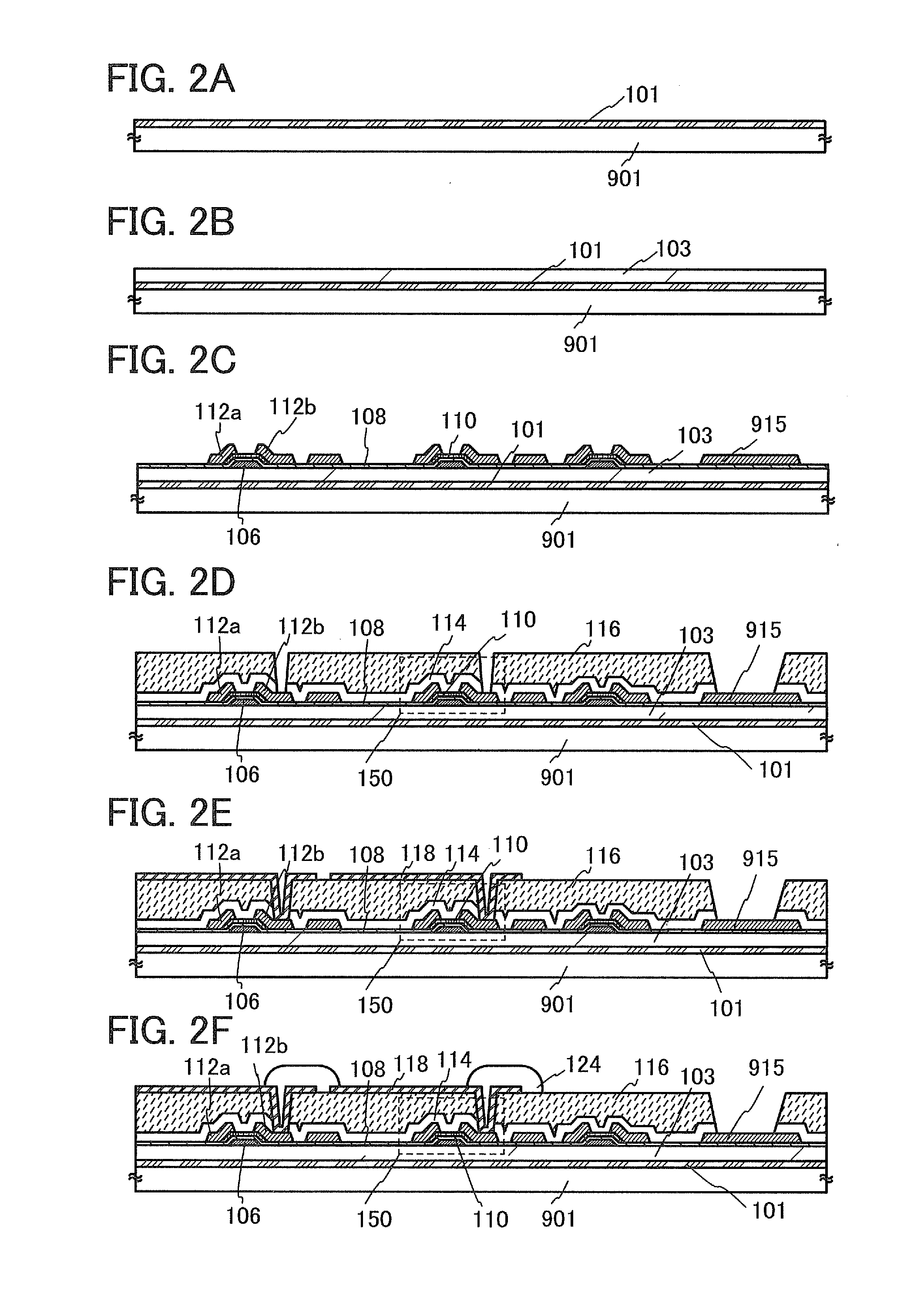
[0038]As shown in FIG. 1B, the light-emitting device includes, in the pixel portion 4502, a third substrate 903, a second adhesive layer 172, a separation layer 101, a buffer layer 103, a plurality of transistors, an insulating layer 114, a planarizing layer 116, a light-emitting element 130, a partition wall 124, a first adhesive layer 171, and a second substrate 902.
[0039]As shown in FIG. 1B, the plurality of transistors is provided over the third substrate 903, and the light-emitting element 130 is provided over each of a transistor 150 and a transistor 151. Each transistor includes a gate electrode layer 106, a source electrode layer 112a, a drain elec...
embodiment 2
[0128]In this embodiment, an oxide semiconductor which can be used for the semiconductor layer in Embodiment 1 will be described in detail.
[0129]For example, an In-based metal oxide, a Zn-based metal oxide, an In—Zn-based metal oxide, or an In—Ga—Zn-based metal oxide can be used as the oxide semiconductor. Alternatively, a metal oxide including another metal element instead of part or all of Ga in the In—Ga—Zn-based metal oxide may be used.
[0130]As the aforementioned another metal element, a metal element that is capable of combining with more oxygen atoms than gallium can be used, for example, and specifically one or more elements of titanium, zirconium, hafnium, germanium, and tin can be used, for instance. Alternatively, as the aforementioned another metal element, one or more elements of lanthanum, cerium, praseodymium, neodymium, samarium, europium, gadolinium, terbium, dysprosium, holmium, erbium, thulium, ytterbium, and lutetium may be used. These metal elements function as a...
embodiment 3
[0144]In this embodiment, a structural example which can be used for the light-emitting element 130 in Embodiment 1 will be described in detail.
[0145]The light-emitting element 130 illustrated in FIG. 13A has a structure in which the organic compound-containing layer 120 is sandwiched between the pair of electrodes (the first electrode layer 118 and the second electrode layer 122). Note that the first electrode layer 118 is used as an anode and the second electrode layer 122 is used as a cathode as an example in the following description of this embodiment.
[0146]The organic compound-containing layer 120 includes at least a light-emitting layer and may have a stacked-layer structure including a functional layer other than the light-emitting layer. As the functional layer other than the light-emitting layer, a layer containing a substance having a high hole-injection property, a substance having a high hole-transport property, a substance having a high electron-transport property, a s...
PUM
 Abstract
Description
Claims
Application Information