Photonic integrated circuits based on quantum cascade structures

Active Publication Date: 2014-01-30
PENDAR TECH LLC +1
View PDF17 Cites 19 Cited by
  • Summary
  • Abstract
  • Description
  • Claims
  • Application Information

AI Technical Summary

Benefits of technology

[0016]Protons or other ions can be implanted into other layers of the structure other than the quantum cascade layer. Lower cladding and upper cladding layers in the passive portion of the multi-layer structure, for example, may be ion-implanted to deplete free charge carriers and reduce optical losses due to those layers. Ion implantation may be performed in stages, and these stages may be interspersed with stages of structure formation. For example, ions can be implanted into the lower cladding and quantum cascade layers in the passive portion of the structure, followed by forming the upper cladding and contact layers. For example, one ion implantation stage can be completed after forming the lower cladding and quantum cascade layers, and additional ions may b

Problems solved by technology

Fabrication methods that have been used for near infrared (NIR) photonic integrated circuits (PICs) are inapplicable or undesirable as to quantum cascade (QC) structures.
For example, increasing the bandgap energy between a conduction band and a valence band does not necessarily prevent inter-subband transitions and accompanying losses within the conduction band for QC structures.
Moreover, NIR PICs fabricated by increasing the bandgap in the passive portion still suff

Method used


Image

  • Photonic integrated circuits based on quantum cascade structures
  • Photonic integrated circuits based on quantum cascade structures
  • Photonic integrated circuits based on quantum cascade structures

Examples


example process # 1

Example Process #1: Single-Schedule Proton Implantation

[0095]An example of a processing sequence that involves a single implantation schedule of proton implantation is described. As shown in FIG. 7A, #1, after growth of the completed QC epitaxial structure and after any high-temperature process such as material re-growth to create buried heterostructure devices, the plasmon / contact layer 617 is etched away in the passive portion of the structure, and a schedule of proton implantation is executed in the passive portion of the multi-layer structure intended to become a passive waveguide. In other embodiments, the Plasmon / contact layers are not removed. Since protons can be implanted very deeply, the optical waveguide can substantially be converted to have low loss through the depletion of electronic carriers.

[0096]Alternatively, the implantation schedule can proceed with the plasmon / contact layers intact, but then these layers can be removed during a subsequent etching process. In oth...

example process # 3

Example Process #3: Fe Implantation Plus Fe:InP Re-Growth

[0102]A third example process sequence, shown in FIG. 7C, involves an Fe implantation schedule 624 and subsequent re-growth 626 of Fe:InP upper cladding layers. Example Process #3 is similar to Example Process #2 in that the QC epitaxial material is grown up through the active layer 613, but prior to growing the upper cladding layer 614. In the passive portion of the structure, where the passive waveguide will be fabricated, a first Fe implantation schedule 624 is performed to deposit Fe ions into the active and lower cladding layers 613 and 615, respectively, in the passive portion of the structure. Then the upper cladding 614 for the QC structure is re-grown. In the passive portion of the structure corresponding to passive waveguide, these active and lower cladding layers 613 and 615 are removed and Fe:InP 626 is re-grown to serve as the upper cladding in the passive portion of the structure. Since the plasmon / contact layer ...

example process # 4

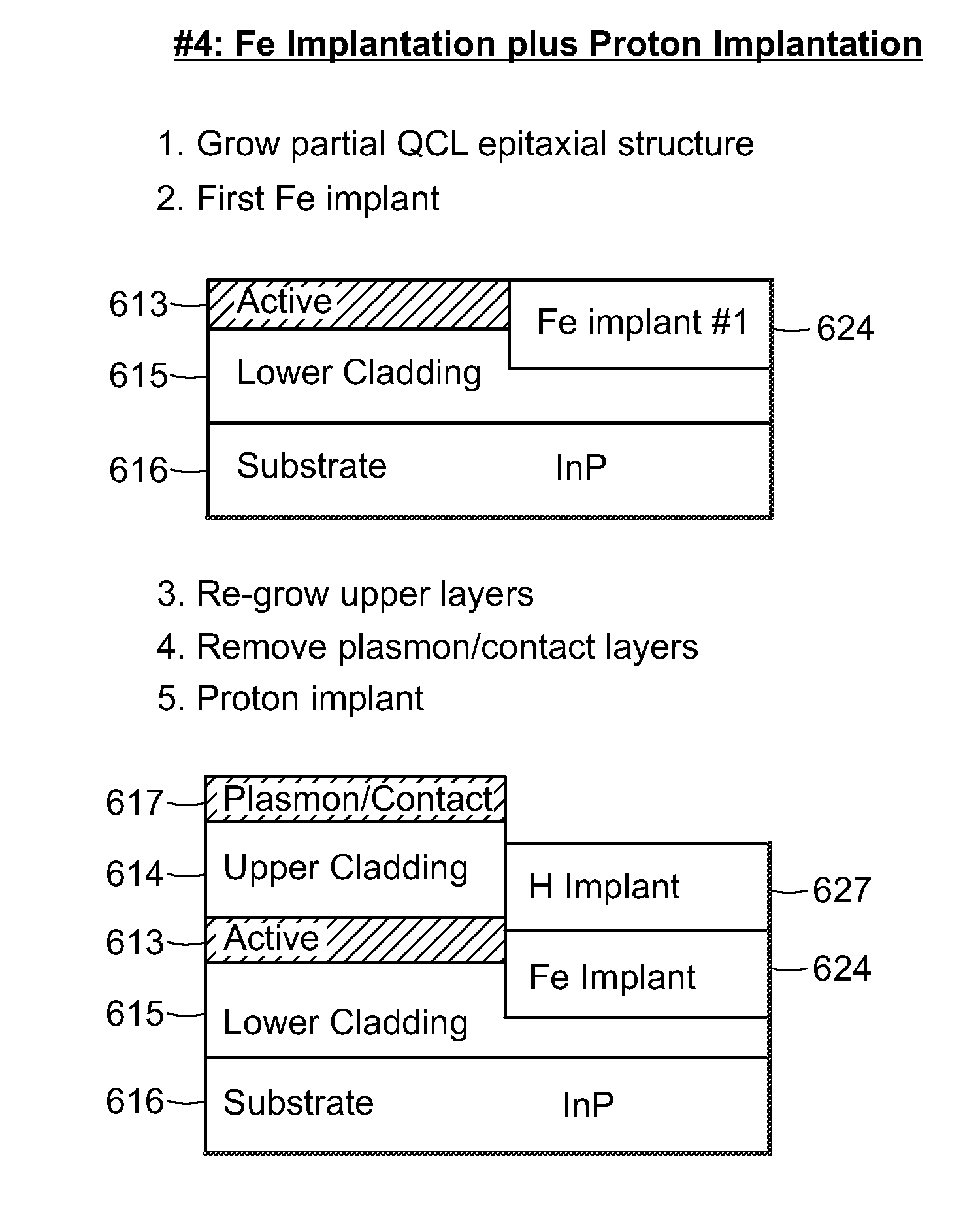
Example Process #4: Fe Implantation Plus Proton Implantation

[0104]A fourth example process sequence, shown in FIG. 7D, involves both Fe and proton implantation. Example Process #4 is similar to Example Process #2 in that the QC epitaxial material is grown up through the active layer 613, but implantation is performed prior to completing growth of the upper cladding layer 614. In the passive portion of the structure, where a passive waveguide will be fabricated, a first Fe implantation schedule 624 is performed to deposit Fe ions into the active and lower-cladding layers 613 and 615, respectively. Then the upper layers 614 and 617 are re-grown and the plasmon / contact layer 617 is etched away in the passive portion of the structure. Following the etching, protons are implanted into the upper cladding layer 614 to convert the layer into low-loss material in the passive portion of the structure. In other embodiments, it is desirable to implant protons through the entire waveguiding regi...


PUM


Abstract

Photonic integrated circuits (PICs) are based on quantum cascade (QC) structures. In embodiment methods and corresponding devices, a QC layer in a wave confinement region of an integrated multi-layer semiconductor structure capable of producing optical gain is depleted of free charge carriers to create a low-loss optical wave confinement region in a portion of the structure. Ion implantation may be used to create energetically deep trap levels to trap free charge carriers. Other embodiments include modifying a region of a passive, depleted QC structure to produce an active region capable of optical gain. Gain or loss may also be modified by partially depleting or enhancing free charge carrier density. QC lasers and amplifiers may be integrated monolithically with each other or with passive waveguides and other passive devices in a self-aligned manner. Embodiments overcome challenges of high cost, complex fabrication, and coupling loss involved with material re-growth methods.

Description

RELATED APPLICATION(S)[0001]This application claims the benefit of U.S. Provisional Application No. 61 / 675,864, filed on Jul. 26, 2012, and U.S. Provisional Application No. 61 / 782,639, filed on Mar. 14, 2013. The entire teachings of the above applications are incorporated herein by reference.GOVERNMENT SUPPORT[0002]The invention described herein was developed jointly by MIT Lincoln Laboratory and Eos Photonics under Navy STTR program N11A-011-0089. The government has certain rights in the invention.BACKGROUND[0003]Photonic integrated circuits (PICs) based on near-infrared (NIR) light include active and passive portions of a single chip and are used to produce off-the-shelf integrated devices. NIR PICs typically incorporate diode lasers, which are bipolar devices that utilize interband transitions between the valence and conduction bands. Diode lasers consist of both n- and p-type layers, and the emission wavelength is directly related to the bandgap of the active regions in the semi...

Claims


Application Information

Patent Timeline
IPC IPC(8): H01L29/15
CPCH01L29/15H01S5/3402B82Y20/00H01S5/026H01S5/2018H01S5/2063H01S5/2275H01S5/3013
Inventor GOYAL, ANISH K.DIEHL, LAURENTPFLUEGL, CHRISTIANWANG, CHRISTINE A.WITINSKI, MARK FRANCIS
Owner PENDAR TECH LLC
Why Eureka
Try Eureka