Methods, process and fabrication technology for high-efficiency low-cost crystalline silicon solar cells

a crystalline silicon, low-cost technology, applied in the direction of chemistry apparatus and processes, final product manufacturing, basic electric elements, etc., can solve the problems of limiting the application of anodic oxidation as a replacement, the incompatibility of anodic oxidation with metallization schemes, and the inability to meet the requirements of metallization, etc., to achieve adequate resistivity, high efficiency, and high transparency

Active Publication Date: 2014-03-06
SPECIAL MATERIALS RES & TECH
View PDF4 Cites 29 Cited by
  • Summary
  • Abstract
  • Description
  • Claims
  • Application Information

AI Technical Summary

Benefits of technology

[0063]It is a further object according to one or more embodiments to provide a process, design, and technology for fabricating high efficiency, low-cost, amorphous silicon solar cells that incorporate the RTWCG SiOM TCO feature.
[0064]It is a further object according to one or more embodiments to provide planar silicon-based electronic and photonic (optoelectronic) device applications that can benefit from the n+ / p-Si or p+ / n-Si RTWCG SiOx ARC / SE( / TO) method, process, and technology from the incorporation of low to medium-high dielectric constant RTWCG SiOx thin film dielectrics, or of high transparency, adequate resistivity, and relatively low reflectance RTWCG SiOM TCO's.

Problems solved by technology

Unfortunately, anodic oxidation is not compatible with metallization schemes, limiting its application as a replacement of thermal grown or CVD deposited SiO2.
One of the major disadvantages of the SiO2 LPD method described above is a very low deposition rate.
These deposition rates are far too low for practical ARC applications; it would require more than one hour to deposit a nearly optimal ARC thickness of 130 nm for solar cell applications.
But even if the simulated reflectance is achieved, the reflective losses are still too high at 10.4% reflectivity.
However, this approach becomes cost prohibitive for most commercial solar cell applications.
Depositing uniform ARCs on textured surfaces is problematic.
The nanometer-sized features of a polysilicon structure make it difficult to deposit or grow uniform ARC through conventional techniques.
Certain cell manufacturers do not use an ARC due to this issue; the penalty they pay is up to a 10% relative loss in efficiency along with surface stability problems.
However, emitters of this type have low open-circuit voltages (high surface recombination for emitters with high surface doping and Auger recombination) as well as poor short-circuit currents due to a poor blue response (high-emitter recombination and free-carrier absorption).
In the case of screen-printing, a selective emitter is difficult to achieve especially through a one-step process.
There has been a delay-in-implementation of the very important SE efficiency enhancement feature because this selectively-patterned emitter doping profile has historically been obtained using expensive photolithographic or advanced screen-printed alignment techniques along with multiple high-temperature diffusion steps
Techniques (a) and (b) are generally time consuming and somewhat expensive.
Although these and other laboratory cell designs have been pushing up the efficiency of c-Si solar cells, to date, none of these cell designs use, low-cost, solar-grade silicon substrates, and only few of them use low-cost fabrication technology process steps such as screen printing metallization.

Method used


Image

  • Methods, process and fabrication technology for high-efficiency low-cost crystalline silicon solar cells
  • Methods, process and fabrication technology for high-efficiency low-cost crystalline silicon solar cells
  • Methods, process and fabrication technology for high-efficiency low-cost crystalline silicon solar cells

Examples


example 1

Ultra-Low Cost RTWCG SiOX Solution

[0322]Ultra-low cost RTWCG SiOx aqueous solution formulations using diluted chemistries are preferably produced on site at the fabrication facility. This not only significantly reduces the cost of H2SiF6, H2TiF6, and other solution components but will maximize the manufacturer's quality control.

[0323]In a preferred embodiment of the invention, the RTWCG SiOx growth solution formulation eliminates the need for a silicon source, such as H2SiF6 or any other silicon source found in the prior art RTWCG SiOX growth solution formulations. ACS grade, or higher grade, HF(conc) and ultra-high purity water can be used to dilute the concentrated HF solution to the desired 10% to 40% concentration. ACS or better grade HCl(conc) also can be used and diluted to desired concentrations. The RTWCG SiOX growth solution also includes non-invasive aqueous components to which small amounts, 1-10 g per 1 L HF(aq), of a single preferred catalyst or a combination of preferr...

example 2

In Situ Surface Cleaning and Compatibility with Screen Printing Metallization

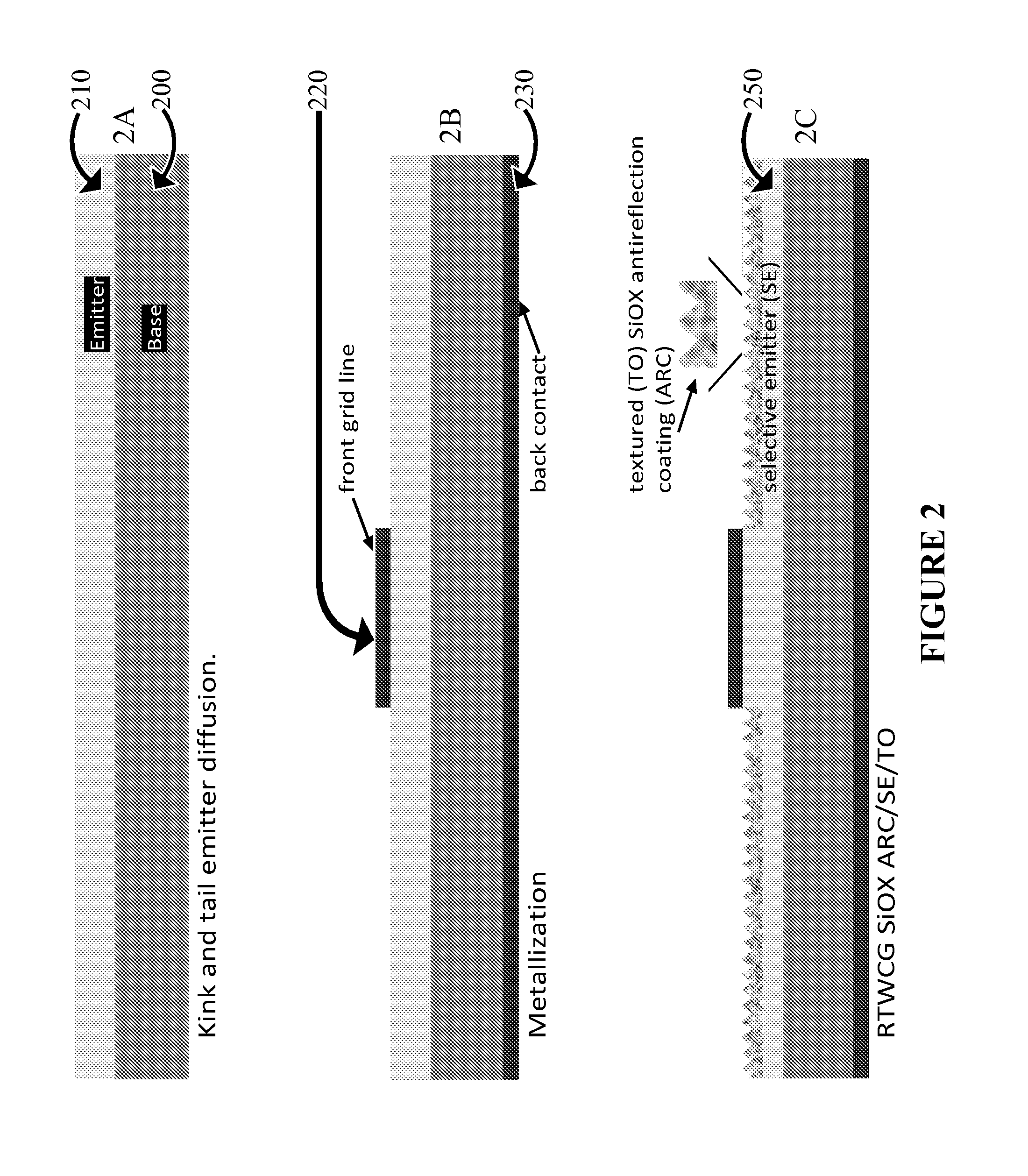
[0325]All experimental small area high efficiency cells are fabricated in clean room facilities, yet most of the current state-of-the-art solar cell manufacturing is conducted in non-clean room environments. Non-clean room environments negatively affect the efficiency of cells by introducing impurities on the cell surface. The RTWCG SiOx ARC / SE process, being the last fabrication step, recaptures the efficiency that is lost due to non clean room environments by cleaning the active surfaces and screen printed front grid lines. Moreover, as can be seen in the examples of realization below, the in situ cleaning lowers the efficiency dispersion within the same batch as well as between batches.

[0326]FIG. 21(a) shows the Nomarski view a c-Si solar cell with a pyramid-textured front surface which had a high peak-to-valley aspect ratio of 25 μm. As can be seen in FIG. 21(b), the RTWCG SiOx process is fully compatib...

example 3

RTWCG SiOx ARC

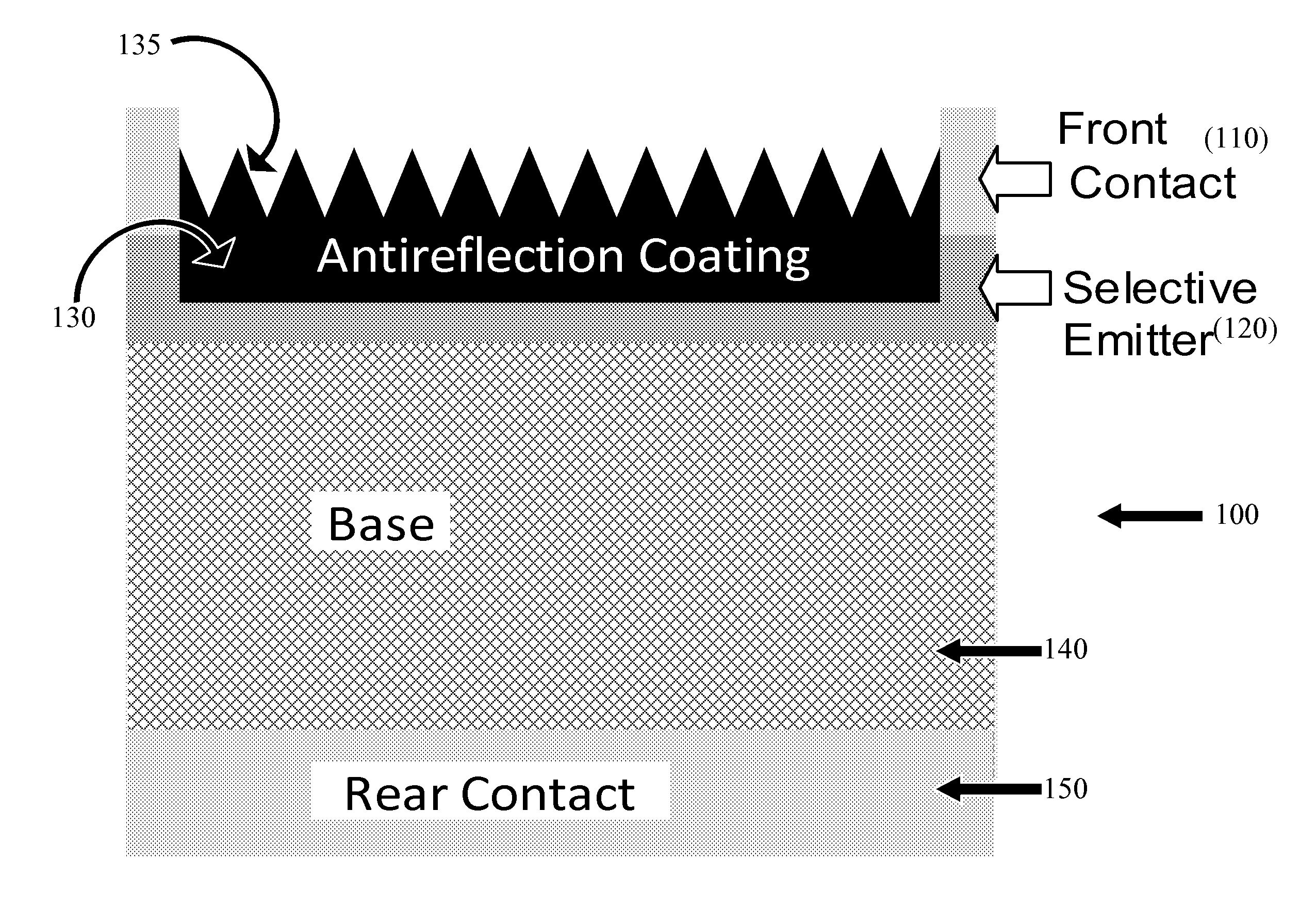
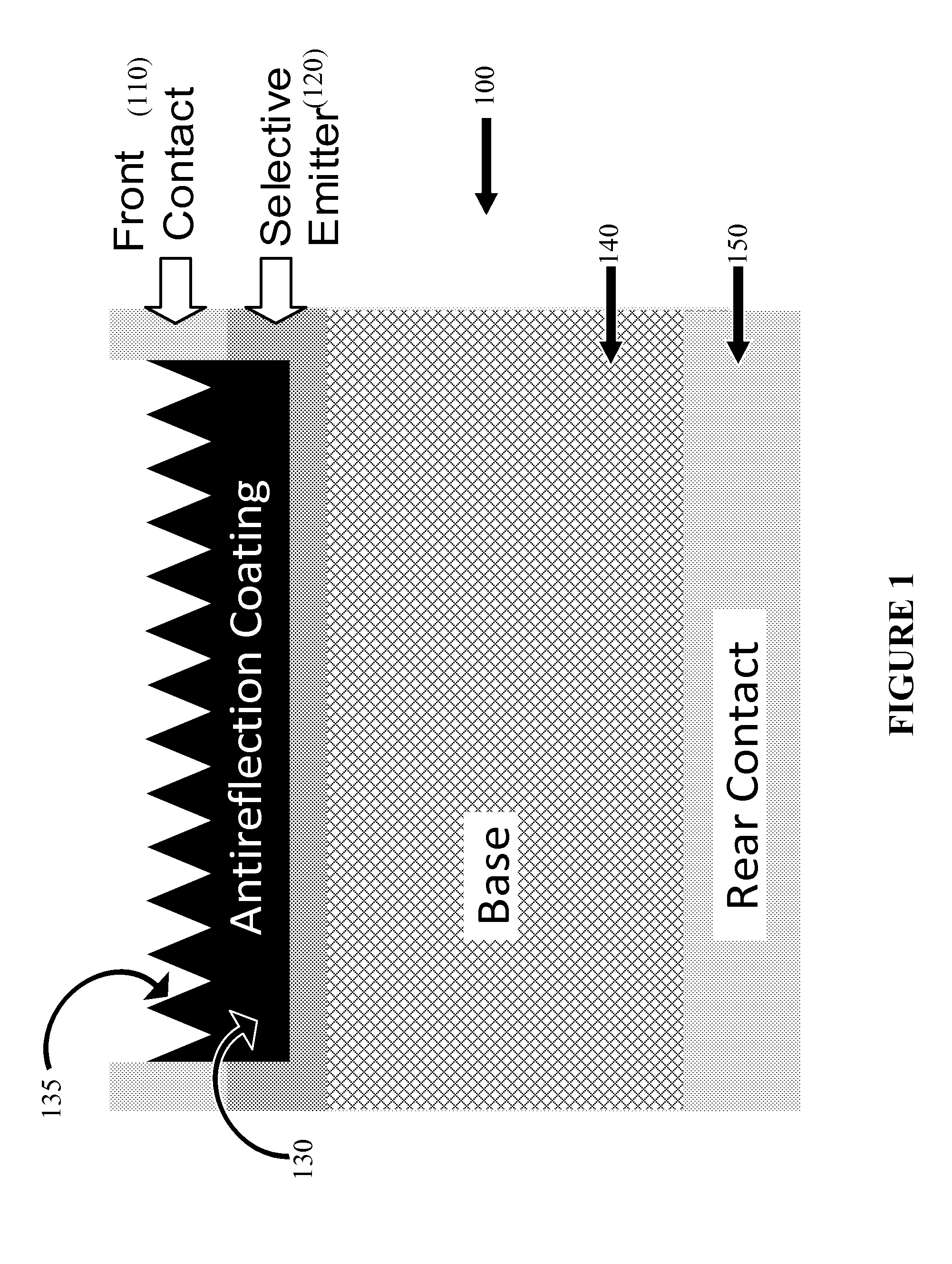
[0334]The efficiency of a solar cell is in large measure determined by its reflectance, and hence, its ability to retain rather than reflect solar energy back into space. Many solar cell manufacturers still use titanium dioxide (TiOx) as a single layer antireflection coating (SLARC), which is usually spray coated onto the cells, then baked in order to eliminate the solvents. The main drawback of the relatively low cost TiOx ARC is the fact that it has a relatively large, ˜15%, AM 1.5 AWR. Additionally, TiOx films cover the front surface metallization, requiring it to be removed from the front bus bars to allow for cell interconnection into lines during solar modules fabrication.

[0335]Silicon Nitrate (SiNx) ARCs are a better approach since their AM1.5 AWR is ˜12%. SiNx is deposited by chemical vapor deposition (CVD), or plasma enhanced CVD (PECVD) at relatively low temperatures in air or vacuum. SiNx deposition is rather expensive from a process, maintenance, and especi...


PUM

PropertyMeasurementUnit
thicknessaaaaaaaaaa
temperaturesaaaaaaaaaa

Abstract

Disclosed is a method, process, solar cell design, and fabrication technology for high-efficiency, low-cost, crystalline silicon (Si) solar cells including but not restricted to solar grade single crystal Si (c-Si), multi-crystalline Si (mc-Si), poly-Si, and micro-Si solar cells and solar modules. The RTWCG solar cell fabrication technology creates a RTWCG SiOx thin film antireflection coating (ARC) with a graded index of refraction and a selective emitter (SE). The resulting top surface of the SiOx oxide can be textured (TO) concomitant with the growth process or through an additional mild wet chemical step.

Description

RELATED APPLICATIONS[0001]The application claim priority under 35 USC §119(e) to U.S. Ser. No. 61 / 383,435, filed Sep. 16, 2010 and entitled “Method, Process And Fabrication Technology For High-Efficiency Low-Cost Crystalline Silicon Solar Cells,” which is hereby incorporated in its entirety by reference.INCORPORATION BY REFERENCE[0002]All patents, patent applications and publications cited herein are hereby incorporated by reference in their entirety in order to more fully describe the state of the art as known to those skilled therein as of the date of the invention described herein.RELATED FIELD[0003]This invention relates to a Room Temperature Wet Chemical Growth (RTWCG) method and process of SiOx thin film coatings which can be grown on various substrates. The invention further relates to RTWCG method and process suited to grow thin films on the Si substrates used in the manufacture of silicon-based electronic and photonic (optoelectronic) device applications. The invention furt...

Claims


Application Information

Patent Timeline
Patent Type & Authority Applications(United States)
IPC IPC(8): C09K13/08H01L31/0216
CPCH01L31/02168C09K13/08H01L31/022425H01L31/02363H01L31/068H01L31/1804H01L31/1868Y02E10/52Y02E10/547H01L31/056Y02P70/50C03C17/25C23F1/16H01L31/02366
Inventor FAUR, MARIAFAUR, HORIA M.FAUR, MIRCEA
Owner SPECIAL MATERIALS RES & TECH
Why Eureka
Try Eureka