Semiconductor device and semiconductor integrated circuit device using the same

a technology of semiconductor integrated circuit and semiconductor, which is applied in the direction of semiconductor devices, electrical devices, transistors, etc., can solve the problem that the concentration of p-type impurities in the drift region cannot be increased unilaterally, and achieve the effect of improving the tradeoff relationship between the withstand voltage and the output current density

Inactive Publication Date: 2014-03-13
HITACHI LTD
View PDF0 Cites 4 Cited by
  • Summary
  • Abstract
  • Description
  • Claims
  • Application Information

AI Technical Summary

Benefits of technology

[0015]The semiconductor device and the semiconductor integrated circuit device using the same according to the present invention can realize the higher concentration and higher withstand voltage of the drift region that extends from the drain region toward under the gate electrode by the above solution to the problem.
[0016]For example in a circuit of FIG. 2, when the p-type MOSFET of the highside is off, and the n-type MOSFET of the lowside is on, a positive supply voltage is ap...

Problems solved by technology

That is, the impurity concentration of the drift region has a trade-off relationship with the withstand voltage and th...

Method used


Image

  • Semiconductor device and semiconductor integrated circuit device using the same
  • Semiconductor device and semiconductor integrated circuit device using the same
  • Semiconductor device and semiconductor integrated circuit device using the same

Examples


first embodiment

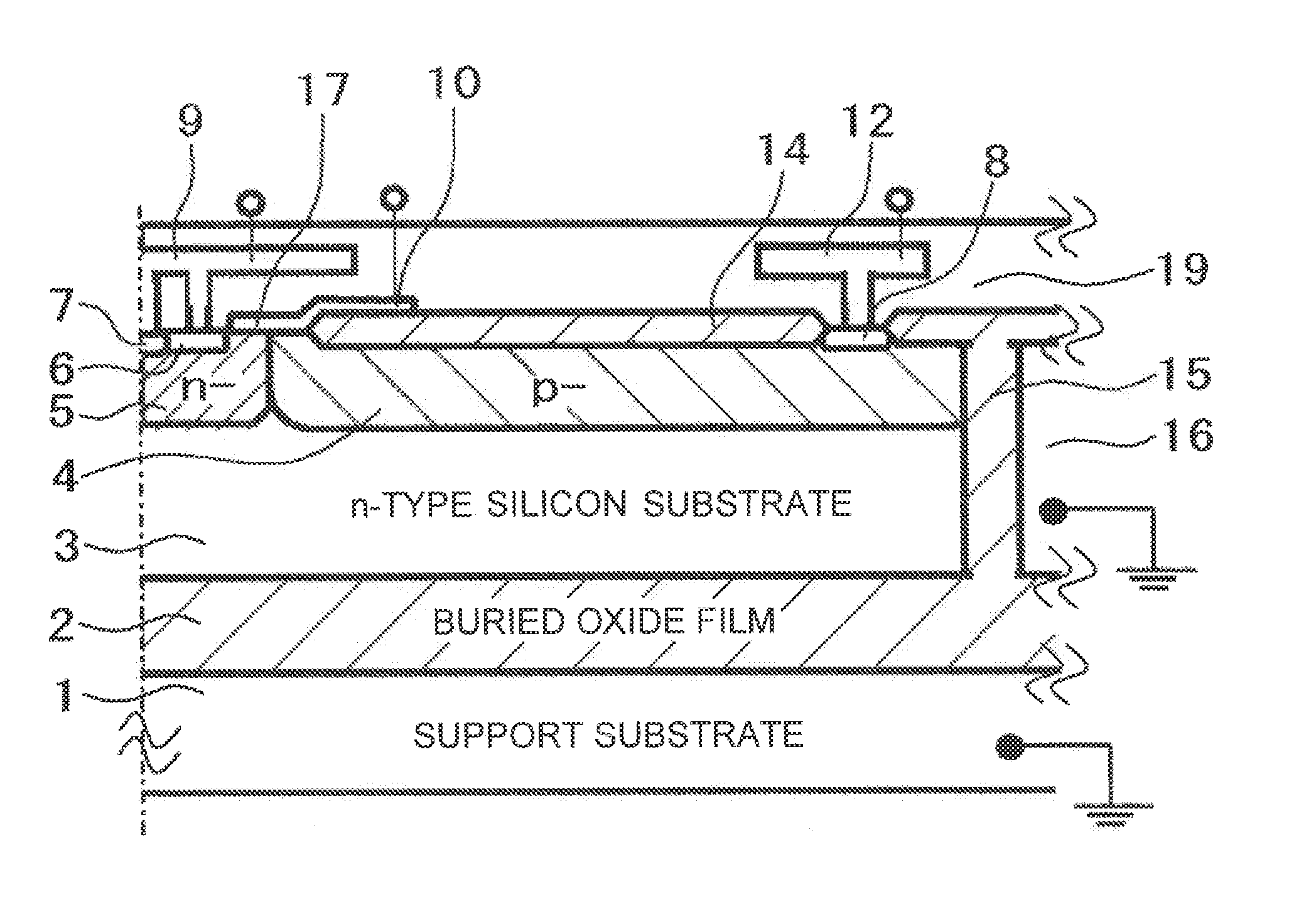
[0028]Hereinafter, a first embodiment of the present invention will be described in detail with reference to the attached drawings. FIG. 1 is a partially cross-sectional structural view illustrating a horizontal p-type MOSFET according to the first embodiment of the present invention. Referring to FIG. 1, the horizontal p-type MOSFET according to the present invention is structured bilaterally symmetrically, and a right half of the structure is illustrated, and a left half thereof is omitted from the figure.

[0029]Referring to FIG. 1, a support substrate 1 formed of a p-type or an n-type silicon substrate, and an n-type semiconductor substrate 3 are isolated from each other by a buried oxide film 2. Also, an insulting film 14 thicker than a gate insulating film 17 and is formed of an oxide film or the like is selectively formed on a surface layer of the n-type semiconductor substrate 3. The insulting film 14 formed of the oxide film or the like corresponds to LOCOS (local oxidation o...

second embodiment

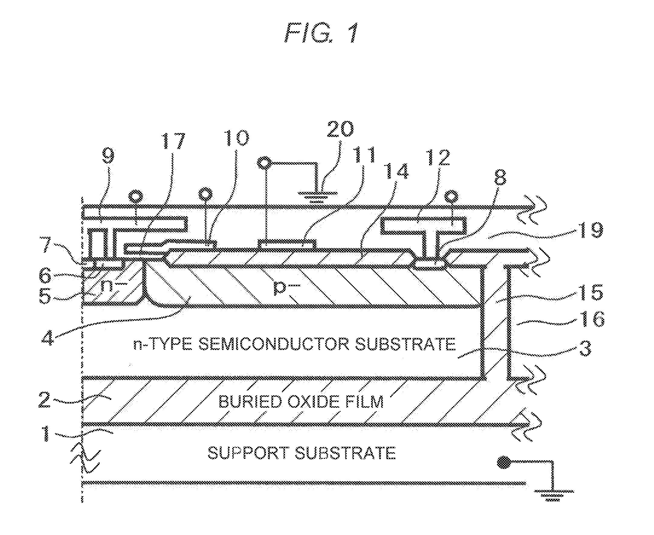
[0045]Subsequently, a second embodiment of the present invention will be described. FIG. 8 is a partially cross-sectional structural view illustrating a horizontal p-type MOSFET according to the second embodiment of the present invention. A difference from FIG. 1 of the first embodiment resides in that a voltage across a power supply 30 for a logic circuit used in the control circuit is applied to the addition electrode. The power supply for the logic circuit is about 5V or 3.3V with respect to the ground, and as compared with the power supply 26 (for example, +50 to 150 V) and the power supply 27 (for example, −50 to 150 V) in FIG. 2, the voltage of −5V to +5V is regarded as substantially the same potential as the ground potential. That is, the power potential of 5V or 3.3V used as the supply voltage for the logic circuit is regarded as substantially the same potential as the ground potential. Therefore, when the voltage of, for example, 5V or 3.3V is applied to the addition electr...

third embodiment

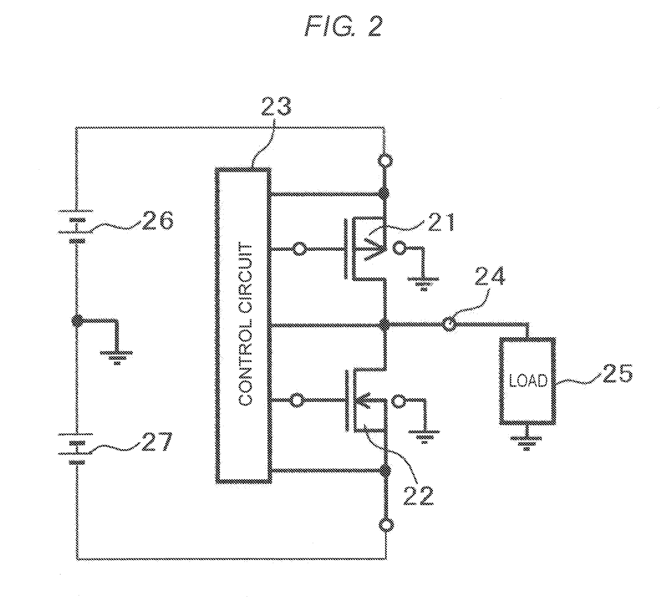
[0046]Subsequently, a third embodiment of the present invention will be described. FIG. 9 illustrates an example of a digital-analog mixed integrated circuit 29 applying the p-type MOSFET according to the present invention. Each of output stage circuits 28 of the digital-analog mixed integrated circuit 29 is the bridge circuit using the p-type MOSFET 21 and the n-type MOSFET 22 illustrated in FIG. 2. Each of the output stage circuits 28 is subjected to on / off control by the control circuit 23 to output the voltage waveform of FIG. 3. Also, the control circuit 23 controls the on / off operation of the respective output stage circuits 28 according to a control signal from the a host control circuit 31, and also transmits a result obtained by measuring a voltage across the terminal 24 to the host control circuit 31. The p-type MOSFET of the present invention is applied to the digital-analog mixed integrated circuit 29, thereby being capable of downsizing the output stage circuits 28, tha...


PUM


Abstract

There is provided an MOSFET having a large current density, which can be mixed with a logic circuit, and is used in a circuit that conducts the operation of applying a negative voltage to a drain electrode. An electrode surrounded by an insulating film is formed, at an intermediate position of a gate electrode and a drain of the MOSFET formed on an SOI substrate having a drain electrode applied with a negative voltage, and the electrode is connected to the ground to prevent a withstand voltage from being lowered which is caused by an increase in impurity concentration of a drift region. A drift resistance is lowered to improve the current density.

Description

BACKGROUND OF THE INVENTION[0001]1. Field of the Invention[0002]The present invention relates a semiconductor device using an insulated gate called “MOSFET (metal oxide semiconductor field effect transistor)” or “MISFET (metal insulator semiconductor field effect transistor), and semiconductor integrated circuit device using the semiconductor device.[0003]2. Background Art[0004]In recent years, semiconductor integrated circuit. devices large in logic scale have been increasingly developed with a functional aggregation or high functionality. In a field of an analog-digital mixed integrated circuit, an semiconductor integrated circuit device in which a middle or high withstand voltage element of 20V to 600V class are combined with a low is circuit having a CMOS (complementary MOSFET) configuration has been developed for on-vehicle, industrial, and medicinal purpose. The analog-digital mixed integrated circuit of this type has been designed and. developed to customize a function to be ...

Claims


Application Information

Patent Timeline
IPC IPC(8): H01L27/092
CPCH01L27/0922H01L27/1203H01L29/7835H01L29/402H01L29/42316H01L29/7802H01L21/02675
Inventor SHIRAKAWA, SHINJISAKANO, JUNICHI
Owner HITACHI LTD
Why Eureka
Try Eureka