

Surface modification
- Summary
- Abstract
- Description
- Claims
- Application Information
AI Technical Summary
Benefits of technology
Problems solved by technology
Method used
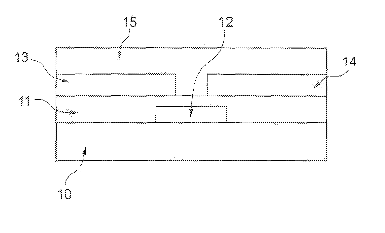
Image

Examples
example 1
[0095]In this example poly(pentafluorostyrene-co-glycidyl methacrylate) was deposited by spin-coating on to a fluorinated polymer surface.
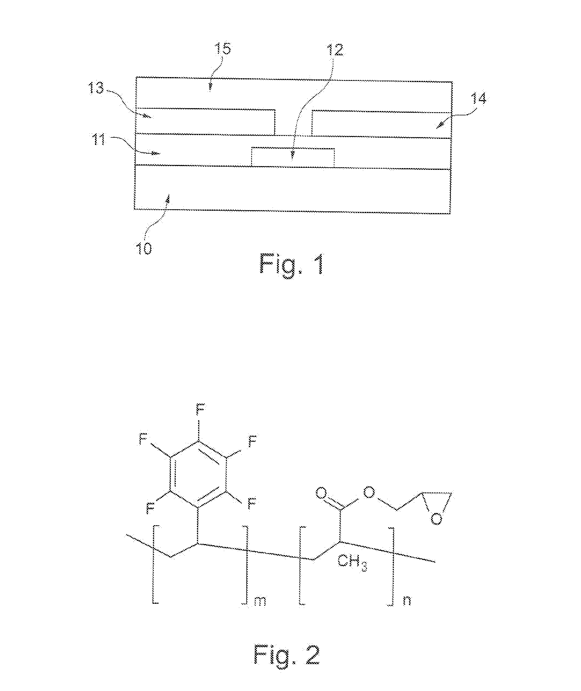
[0096]Poly(pentafluorostyrene-co-glycidyl methacrylate) is a copolymer comprising predominantly pentafluorophenyl groups, the glycidyl methacrylate fraction is only around 10%. The structure of poly(pentafluorostyrene-co-glycidyl methacrylate) is shown in FIG. 2.
[0097]A fluorinated polymer surface was prepared by spin coating a 2% PTFE solution in a 1:1 mixture of FC-70 (perfluorotripentylarine) and FC-75 (perfluoro-2-n-butyl THF) (both supplied by 3M) on to a glass substrate. Spin coating was carried out at 1000 rpm for a period of 20 seconds. This was followed by annealing at 100° C. in air for a period of 10 minutes.
[0098]Three poly(pentafluorostyrene-co-glycidyl methacrylate) solutions were prepared, in which: (i) poly(pentafluorostyrene-co-glycidyl methacrylate) was dissolved in hexafluorobenzene; (ii) poly(pentafluorostyrene-co-glycidyl meth...
example 2
[0107]This example is similar to Example 1 insofar as it involved the deposition of a poly(pentafluorostyrene-co-glycidyl methacrylate) wetting layer on to a fluorinated polymer surface.
[0108]In this example, however, a small non-fluorinated aromatic molecule, namely triisopropylsilylethynyl (TIPS) pentacene, was deposited on to the poly(pentafluorostyrene-co-glycidyl methacrylate) layer. As compared with polystyrene, TIPS pentacene can more easily be observed due to its intense colour and crystallinity.
[0109]In a first experiment, TIPS pentacene dissolved in toluene was spin-coated on to the poly(pentafluorostyrene-co-glycidyl methacrylate) layer at 1000 rpm for a period of 60 seconds.
[0110]Spin-coating of TIPS pentacene from toluene resulted in a thin, faint blue TIPS pentacene film being formed. Localised film defects were observed, possibly due to some dissolution of the poly(pentafluorostyrene-co-glycidyl methacrylate) wetting layer in the TIPS pentacene / toluene solution during...
PUM
 Abstract
Description
Claims
Application Information