
Passive layer for attenuation of near-field electromagnetic waves and heatdissipation including graphene, and electromagnetic device including the same

a near-field electromagnetic wave and heat dissipation technology, applied in the direction of inorganic insulators, insulating bodies, modified by conduction heat transfer, etc., can solve the problem of frequent malfunction of devices without normal operation, interference with each other, and hybridization of dielectric noise-radiating active elements with passive elements, etc. problems, to achieve the effect of reducing noise, reducing interference, and removing hea

Active Publication Date: 2014-08-07
KOREA INST OF SCI & TECH +1
View PDF9 Cites 49 Cited by
  • Summary
  • Abstract
  • Description
  • Claims
  • Application Information

AI Technical Summary

Benefits of technology

The invention is about a flexible film that can block electromagnetic waves and prevent them from interfering with electronic devices. The film is made up of a layers of graphene and insulating material that can be applied to circuit boards, semiconductor devices, or flexible films. This film has high heat dissipation and light transmission properties, making it useful for reducing noise and removing heat in electronic devices. It is also very thin and flexible, making it ideal for use in thin film devices and nanodevices.

Problems solved by technology

Thus, there is a tendency to hybridize dielectric noise-radiating active elements with passive elements.
As a result of this hybridization, capacitive coupling and inductive coupling enhance cross talk, radiated noises interfere with each other, and heat is released, resulting in frequent malfunction of devices without normal operation.
In some cases, noises in the near-field region, i.e., the distance between the radiation source and noise attenuation material is lower than the wavelength of the radiation (λ / 2π), may interfere with each other.
This interference often affects the operation of an external device.
Accordingly, the shielding techniques cannot be used to suppress interference of near-field noises emitted from internal IC chips and circuits of devices.
An excessively high reflectance of noises may also negatively affect peripheral circuits and an excessively high absorbance of noises may lead to signal reduction.
However, the use of these elements is not suitable as an urgent measure against noises in devices with short life cycles because mounting spaces for the elements are required and miniaturization and slimness of the elements should be considered from the design stage.
Inductance elements are also still very insufficient for use in the radio-frequency (RF) or semi-microwave band due to their low-frequency characteristics of the real component of permeability.
However, there are no elements that are convenient to use as measures against noises in the RF band.
Even though some passive elements are known to be suitable as measures against noises, enormous costs are incurred, for example, in changing the design of substrates.
Particularly, methods for noise attenuation using a number of passive elements in devices such as semiconductor devices, smart phones, and flexible displays, which require smaller size and thickness and lighter weight, have difficulties in mounting the passive elements and in achieving slimness and heat dissipation due to the limited sizes of the passive elements.

Method used

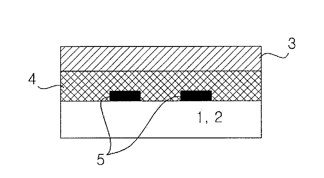
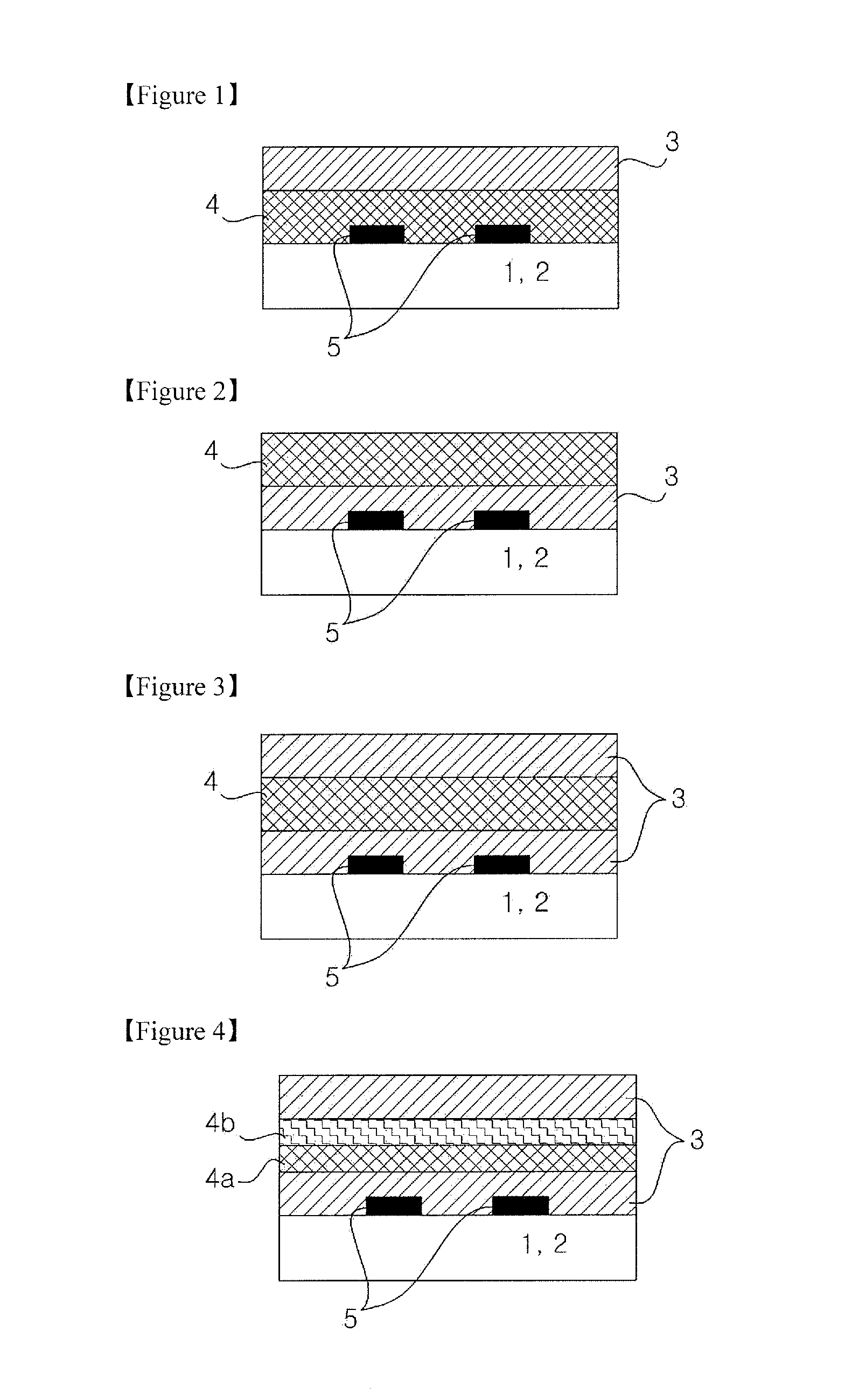
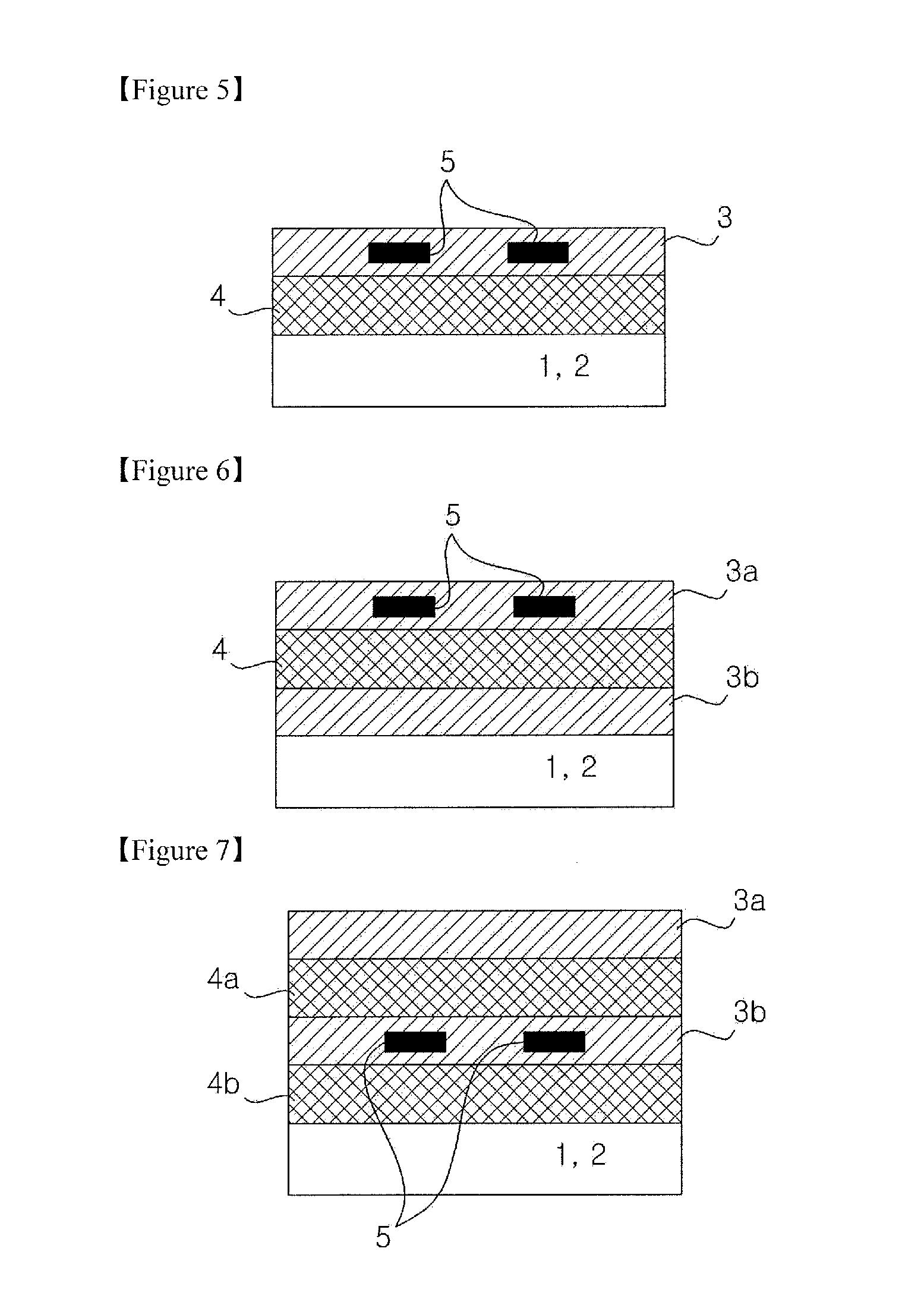

Image

  • Passive layer for attenuation of near-field electromagnetic waves and heatdissipation including graphene, and electromagnetic device including the same
  • Passive layer for attenuation of near-field electromagnetic waves and heatdissipation including graphene, and electromagnetic device including the same
  • Passive layer for attenuation of near-field electromagnetic waves and heatdissipation including graphene, and electromagnetic device including the same

Examples


examples

1. Growth of Large-Area Graphene Layer on Copper Foil

[0087]An about 7.5 inch quartz tube was wrapped with a Cu foil (thickness: 25 μm, size: 210×297 mm2, Alfa Aesar Co.) to form a roll of the Cu foil. The quartz tube was inserted into and fixed to an about 8 inch quartz tube. Thereafter, the quartz tube was heated to 1,000° C. at 180 mTorr under a flow of 10 sccm H2. After the temperature of the quartz tube reached 1,000° C., the quartz tube was annealed for 30 min while maintaining the hydrogen flow and pressure. Subsequently, a gas mixture including a carbon source (CH4:H2=30:10 sccm) was supplied to the quartz tube at 1.6 Torr for 15 min to grow graphene on the Cu foil. The graphene-grown Cu foil was cooled to room temperature at a rate of about 10° C. / s under a flow of H2 at a pressure of 180 mTorr in a short time to obtain a graphene layer grown on the Cu foil.

2. Coating of Graphene Protective Film by Roll-to-Roll Process

[0088]Thereafter, a flexible PET polymer substrate having...


PUM

PropertyMeasurementUnit
Flexibilityaaaaaaaaaa
Attenuation coefficientaaaaaaaaaa
Dielectric constantaaaaaaaaaa

Abstract

The present invention relates to a passive layer including graphene for the attenuation of near-field electromagnetic waves and heat dissipation. The passive layer blocks electromagnetic waves radiated from an external electronic device or prevents electromagnetic waves generated in an electronic device from emitting to the outside. The passive layer is designed to reduce interference between transmission circuits of a device in the near-field region or influence such as malfunction caused by external electromagnetic waves. The present invention also relates to an electromagnetic device and a circuit board, each including the passive layer.

Description

TECHNICAL FIELD[0001]The present invention relates to a passive layer for the attenuation of near-field electromagnetic waves and heat dissipation including graphene, and an electromagnetic device including the passive layer.BACKGROUND ART[0002]In recent years, there has been increasing demands for rapid circuit signal processing, high frequency, high performance, miniaturization, and ultra-slimness of electronic elements in digital devices for various applications, such as automotive vehicles, mobiles, displays, and information electronics. Flexibility is further required in flexible electronic devices. In response to these demands, efforts have been made, for example, to highly integrate circuits in semiconductor devices. Thus, there is a tendency to hybridize dielectric noise-radiating active elements with passive elements. As a result of this hybridization, capacitive coupling and inductive coupling enhance cross talk, radiated noises interfere with each other, and heat is relea...

Claims


Application Information

Patent Timeline
IPC IPC(8): H05K9/00H05K1/02H05K13/00H05K7/20
CPCH05K9/0081H05K7/2039H05K1/0216H05K2201/06H05K13/00H05K2201/0707H05K1/0201B32B9/005B32B9/007B32B9/04B32B9/045B32B2307/206B32B2307/212B32B2457/00C01B32/186C01B32/194H05K9/0088H05K2201/0323B32B9/00H01B3/02H01B17/62H05K9/00
Inventor KIM, SANG WOOHONG, BYUNG HEECHOI, JAEBOONGKANG, JUNMOHWANG, SOON HWI
Owner KOREA INST OF SCI & TECH
Learn More