
Sic crystal with low dislocation density

Active Publication Date: 2014-08-07
SK SILTRON CSS LLC
View PDF5 Cites 20 Cited by
  • Summary
  • Abstract
  • Description
  • Claims
  • Application Information

AI Technical Summary

Benefits of technology

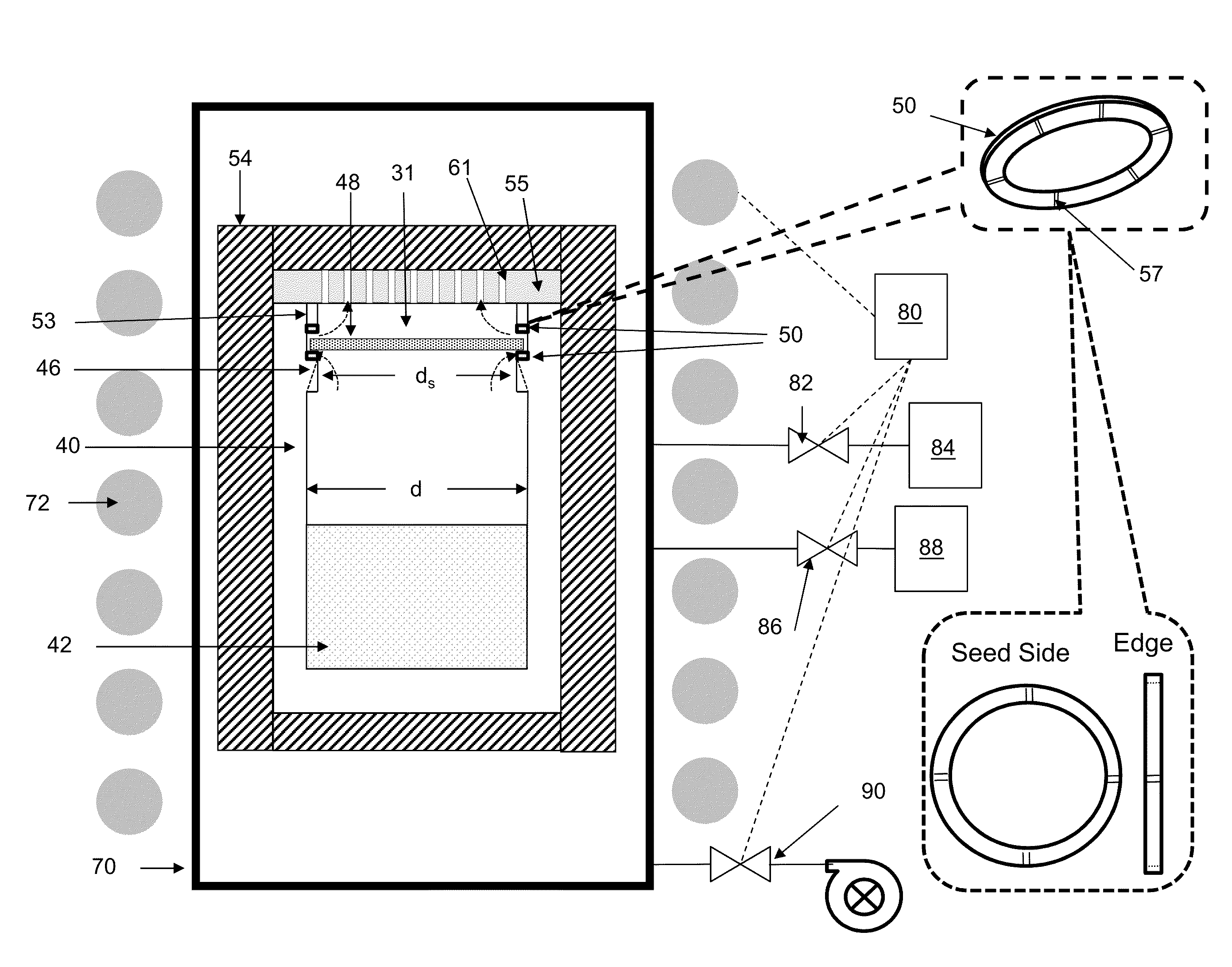
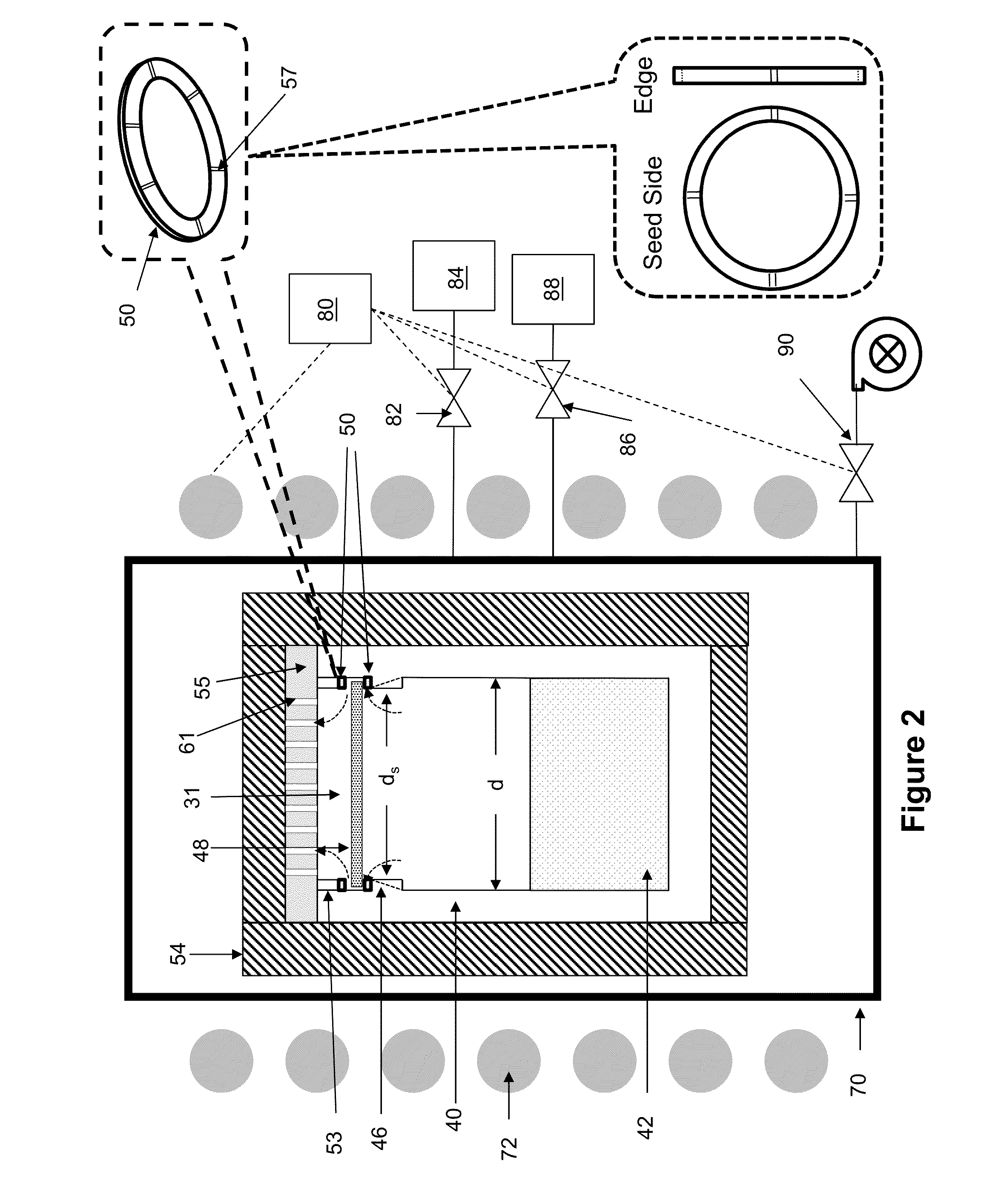
This patent is about a method of growing silicon carbide (SiC) crystals using a vapor transport method. The invention provides support for the seed crystal during the crystal growth process by maintaining the seed crystal in a stress-free state. The method involves placing the seed crystal in a graphite container and adding a source of silicon and carbon atoms for transport to the seed crystal. The container is then placed in a furnace and heated to a high temperature. Evacuation of the furnace is done while gas flows through the seed crystal to facilitate vapor transport without touching the graphite container. The technical effect of this invention is to produce high-quality SiC crystals with improved purity and consistency.

Problems solved by technology

Growth of SiC by sublimation is very challenging.
Temperatures in excess of 2,000° C. are required to generate vapor stream of Si / C species by sublimation, which places great limitations on the reaction cell components and the furnace design.
While this appears simple in concept, in practice the growth of SiC is very complicated and recognized by those who practice as very difficult to perform.
Stresses arising from temperature gradients and thermal expansion mismatch and imparted to the seed and the crystal during growth can result in formation of dislocations.
Deviation of the stoichiometry in the sublimation vapor stream from that needed to form SiC can result in unstable polytype growth—in turn leading to polytype inclusions in the grown crystal, which lead to dislocation formation at the polytype boundaries.
The large count of dislocations makes it very impractical to count every single one, especially as today inspections can be required on sections greater than or equal to the equivalent of 100 mm diameter circles.
However, incorrect sampling methods can lead to errors in the estimation of the dislocation concentration associated with larger crystals.
In most reports, the details of the sampling method are not provided, so replication of reported results can often be difficult, if not impossible.
Scientists experienced in solid state physics and semiconductor devices know that dislocations result in device performance below the theoretical properties of the material.
Due to its hardness, fabrication of SiC into wafer substrates presents unique challenges compared to processing other common semiconductor crystals like silicon or gallium arsenide.
When the tilt is not adequate, the CVD process will produce three dimensional defects on the surface, and such defects will result in non-operational semiconductor devices.
Defects in SiC are known to limit or destroy operation of semiconductor devices formed over the defects.
Neudeck and Powell reported that hollow core screw dislocations (micropipes) severely limited voltage blocking performance in SiC diodes (P. G. Neudeck and J. A. Powell, IEEE Electron Device Letters, vol.
Modern technology for growth of 4H—SiC crystals has not been successful to develop a commercial method for a crystal growth process that allows simultaneous control over the gamut of dislocation types.
Various methods disclosed in the prior art are often lacking detail regarding the specific steps employed in the crystal growth or the methods employed to assess the concentration of defects and demonstrate repeatability.
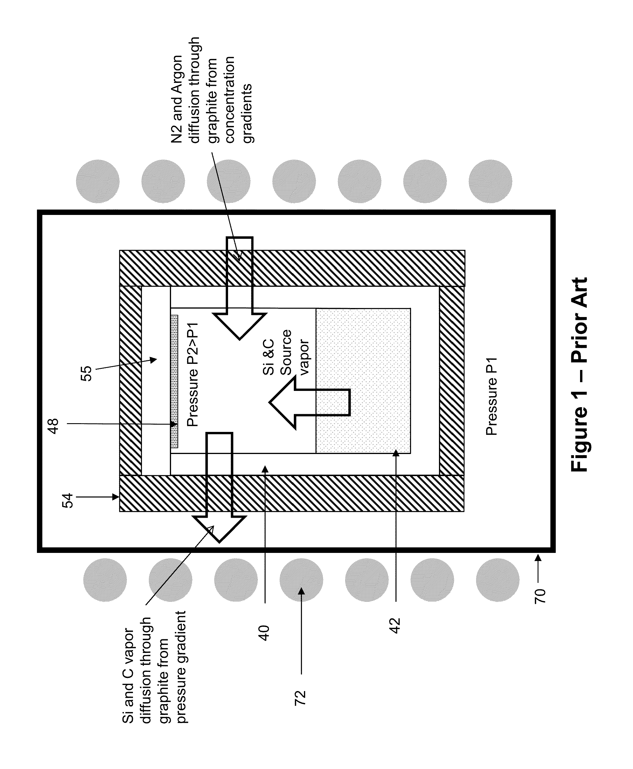
However, the act of mounting the seed to the reaction cell lid or seed holder can lead to undesirable effects during crystal growth.
For example, during the mounting process, scratching of the coated seed back may occur.
In addition, a void may be created between the seed and reaction cell ceiling interface during the mounting process.
Such occurrences may exacerbate formation of evaporation cavities of the seed backside, resulting in defect formation.
Moreover, differences in thermal expansion between the seed and lid can cause stresses in the seed.
However, because the reaction cell is typically made from a different material than the seed crystal, the rigid attachment methods often create stresses in the crystal during growth.
For example, when the seeds are mounted to the reaction cell or lid using an adhesive, it is possible for the seed to be bent during the mounting process, which results in undesirable stress in the crystal.
However, contact between the crystal and holder is such that stress on the crystal may still occur during growth.
Moreover, if the lid's surface is not smooth and flat, it will create pressure points on the back surface of the seed, thereby generating strains in the seed.
Even if the lid is perfectly flat such that the seed perfectly contacts the lid, when seed touches the lid it will cool the backside of the seed, causing it to bow away from the lid and the seal will be broken.
Also, the bowing will cause the crystal to be in stress, leading to defects in the growing crystal.
There are other problems with the approach disclosed in the JP 2011-20860.
For example, when the seed is elevated due to pressure differential, it blocks gas flow out of the crucible, thus leading to increased pressure and temperature inside the crucible.
Also, as the crystal grows it gets heavier and at some point will be too heavy for the pressure differential to maintain it against the lid, at which point the crystal would drop, leading to sudden change in the temperature of the crystal and due to resumed flow of gas out of the crucible, reduced pressure and temperature inside the crucible.

Method used


Image

  • Sic crystal with low dislocation density
  • Sic crystal with low dislocation density
  • Sic crystal with low dislocation density

Examples


example

[0067]A graphite vessel was formed and loaded with a source mixture of silicon and carbon totaling approximately 850 grams. A 4H—SiC seed of approximately 102 mm diameter was fixtured into the cell per the methods described earlier with the C-face facing the source. The graphite assembly was wrapped with graphite felt and placed into a RF induction heated vacuum furnace. The vacuum chamber was evacuated to base pressure and then backfilled with argon gas. The pressure was set to 600 T and the system was heated to achieve a temperature of approximately 2200° C. as read by a pyrometer focused on the lid of the graphite vessel. N2 gas was delivered to the chamber at this time and the pressure was dropped below 10 T to initiate sublimation of the source. The N2 gas flow was set to a level to deliver a nitrogen concentration in the crystal within the range 3-8E18 / cm3. After about 100 hrs the pressure was raised to 600 T to stop sublimation and then the system was cooled to retrieve the c...


PUM

PropertyMeasurementUnit
Temperatureaaaaaaaaaa
Lengthaaaaaaaaaa

Abstract

A method of forming an SiC crystal, the method including: placing a SiC seed in a growth vessel, heating the growth vessel, and evacuating the growth vessel, wherein the seed is levitated as a result of a temperature and pressure gradient, and gas flows from a growth face of the seed, around the edge of the seed, and into a volume behind the seed, which is pumped by a vacuum system.

Description

RELATED APPLICATION[0001]This application claims priority benefit from U.S. Provisional Application No. 61 / 761,179, filed Feb. 5, 2013.BACKGROUND[0002]1. Field[0003]This disclosure relates to production of silicon carbide with low dislocation density count and to method and apparatus for supporting an SiC seed during physical vaport transport growth.[0004]2. Related Art[0005]Silicon carbide, SiC, is a crystalline semiconductor material, recognized by those familiar with materials science, electronics and physics as being advantageous for its wide band gap properties and also for extreme hardness, high thermal conductivity and chemical inert properties. These properties make SiC a very attractive semiconductor for fabrication of power semiconductor devices, enabling power density and performance enhancement over devices made from more common materials like silicon.[0006]The most common forms of SiC consist of cubic or hexagonal arrangements of atoms. The stacking of Si and C layers c...

Claims


Application Information

Patent Timeline
IPC IPC(8): C30B23/02C30B23/00C30B29/36
CPCC30B23/025C30B29/36C30B23/005C30B23/002Y10T428/24355C23C14/0635C23C14/22
Inventor LOBODA, MARK
Owner SK SILTRON CSS LLC
Learn More