Multi-layer flexible circuit board and process for producing the same
- Summary
- Abstract
- Description
- Claims
- Application Information
AI Technical Summary
Benefits of technology
Problems solved by technology
Method used
Image
Examples
first embodiment
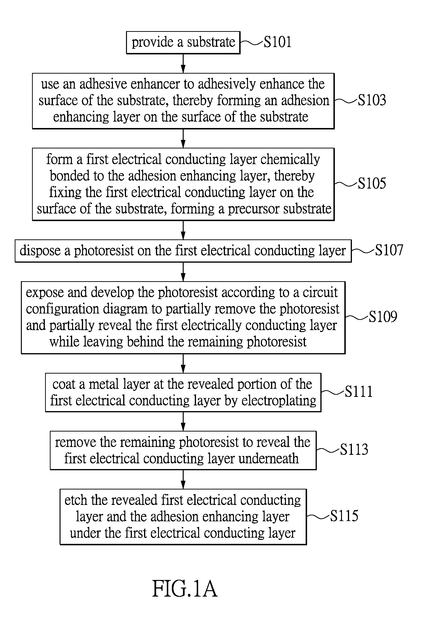
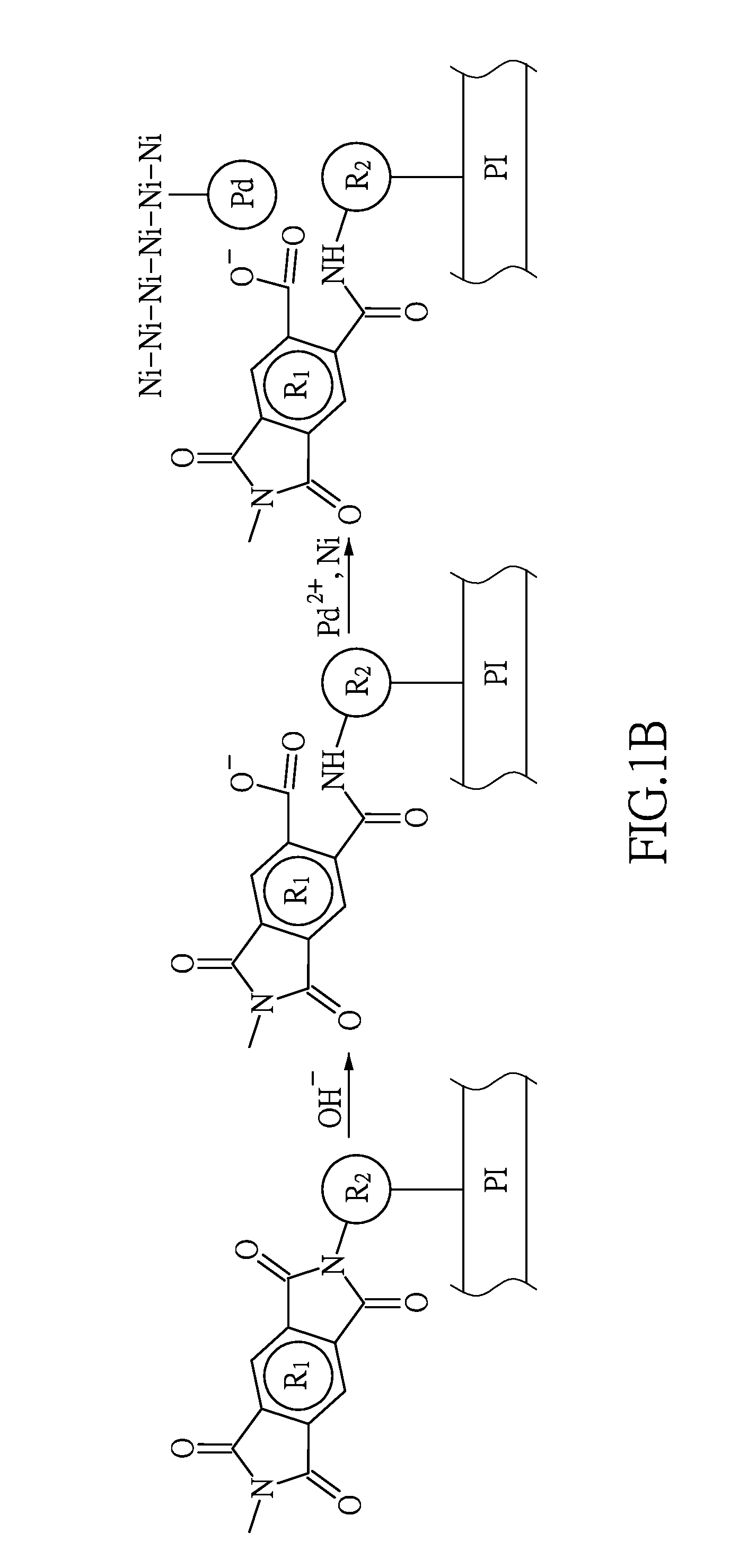
[0020]Referring to FIG. 1A which is a flowchart according to a first embodiment of the present disclosure, the present disclosure provides a process for producing a flexible circuit board, including the following steps.
[0021]As shown in the cross-sectional diagram of FIG. 2A, provide a substrate 10 having a surface 11. The surface 11 of the substrate 10 includes an upper surface 11a and a lower surface 11b. The substrate is a raw material and can be polyimide (PI), polyethylene terephthalate polyester (PET), polyethylene naphthalate (PEN), polytetrafluorethylene (PETE), thermotropic liquid crystal polymer (LCP, epoxy, aramid or other macromolecular polymers. Referring to FIG. 2B, a via hole 12 can be bored by laser beam processing according to need on the substrate 10 interconnecting the upper surface 11a and the lower surface 11b. The via hole 12 has a tunnel wall 121 (step S101). Additionally the substrate 10 processed by laser beam can be cleaned by plasma to remove residue left ...
second embodiment
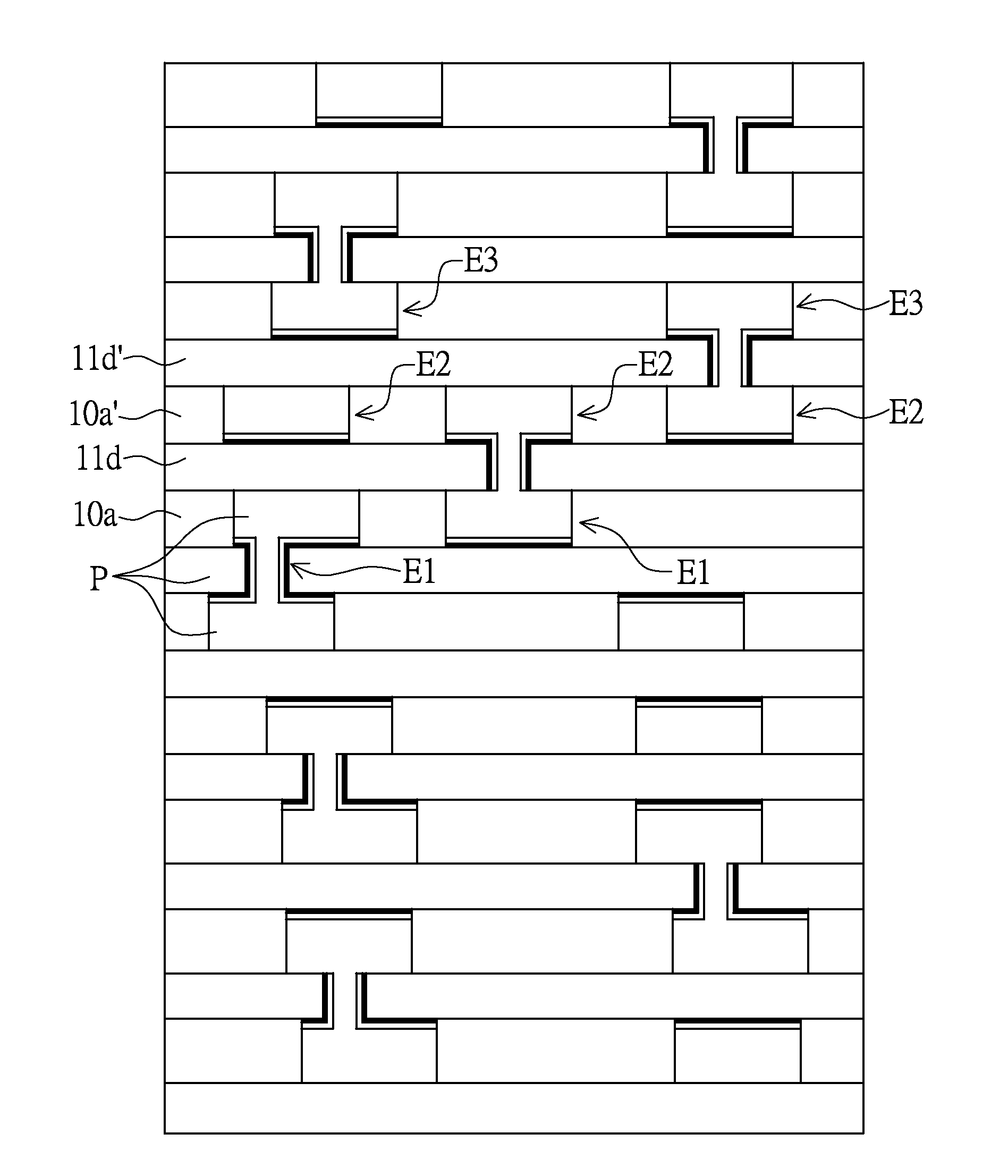
[0040]In another embodiment, as shown in the flowchart of FIG. 3 in conjunction with cross-sectional views of FIG. 4A, FIG. 4B, and FIG. 4C, the present disclosure provides a method of manufacturing a multi-layer flexible circuit board, including the following steps. Provide a flexible circuit board P whose surface 11 includes an upper surface 11a and a lower surface 11b. The surface 11 has a first electric circuit E1 protruding from the surface 11 and an empty portion 11c having no first electrical circuit E1 (step S301). Coat an electric insulation layer on the surface 11 of the flexible circuit board P, such that the electric insulation layer fills up the empty portion 11c to form a neighboring interval layer 10a. The electric insulation layer coats the top portion of the first electric circuit E1, forming a vertical interval layer 11d (step S303) such that the electric insulation layer coats at least two sides of the first electric circuit E1 (step S305).
[0041]Preferably, the el...
third embodiment
[0054]Returning to FIG. 2A, FIG. 2B and FIG. 2C, the present disclosure further provides a precursor substrate (label omitted) as a partially finished product of a circuit board, to be used in subsequent circuit board processing. The precursor substrate includes at least: a substrate 10 and a first electrical conducting layer 30. The substrate 10 has a surface 11 which is adhesively enhanced. The adhesively enhanced surface 11 includes an adhesion enhancing layer 20. The first electrical conducting layer 30 adheres to the adhesion enhancing layer 20 such that the first electrical conducting layer 30 encloses the surface 11 of the substrate 10.
[0055]Preferably, the material of the substrate is polyimide; the adhesion enhancing layer 20 includes a palladium adhesion enhancer; the thickness of the first electrical conducting layer 30 is between 50 and 200 nanometers; and the first electrical conducting layer 30 is an electroless plating layer made of a material selected from the group ...
PUM
| Property | Measurement | Unit |
|---|---|---|
| Thickness | aaaaa | aaaaa |
| Adhesion strength | aaaaa | aaaaa |
| Flexibility | aaaaa | aaaaa |
Abstract
Description
Claims
Application Information


