Plasmonic ir devices

US20140291704A1Active Publication Date: 2014-10-02SCIOSENSE BV

Image

  • Plasmonic ir devices
  • Plasmonic ir devices
  • Plasmonic ir devices

Examples


Embodiment Construction

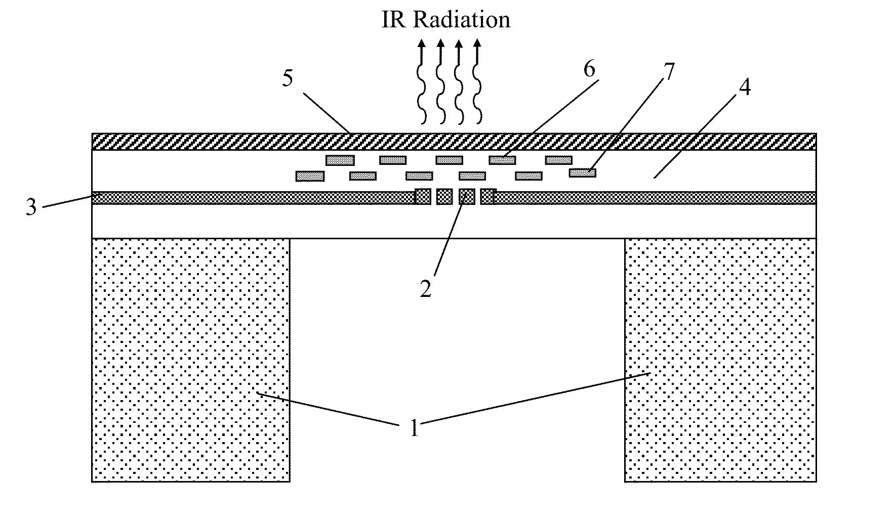
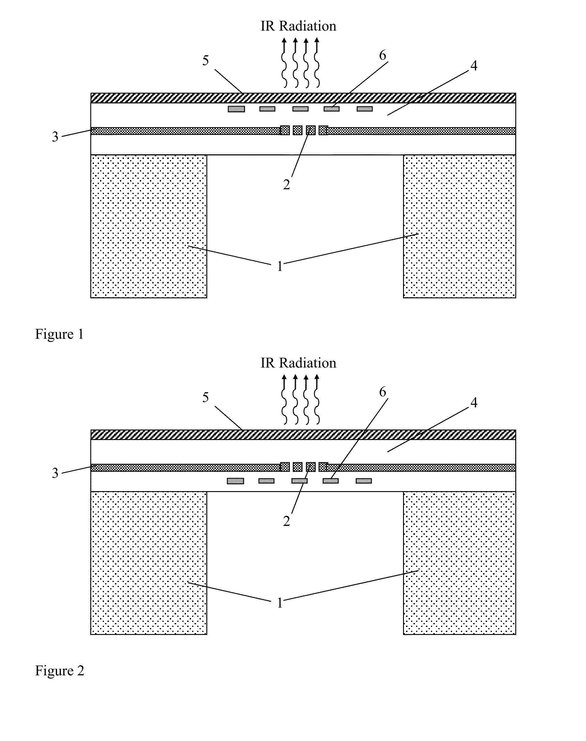
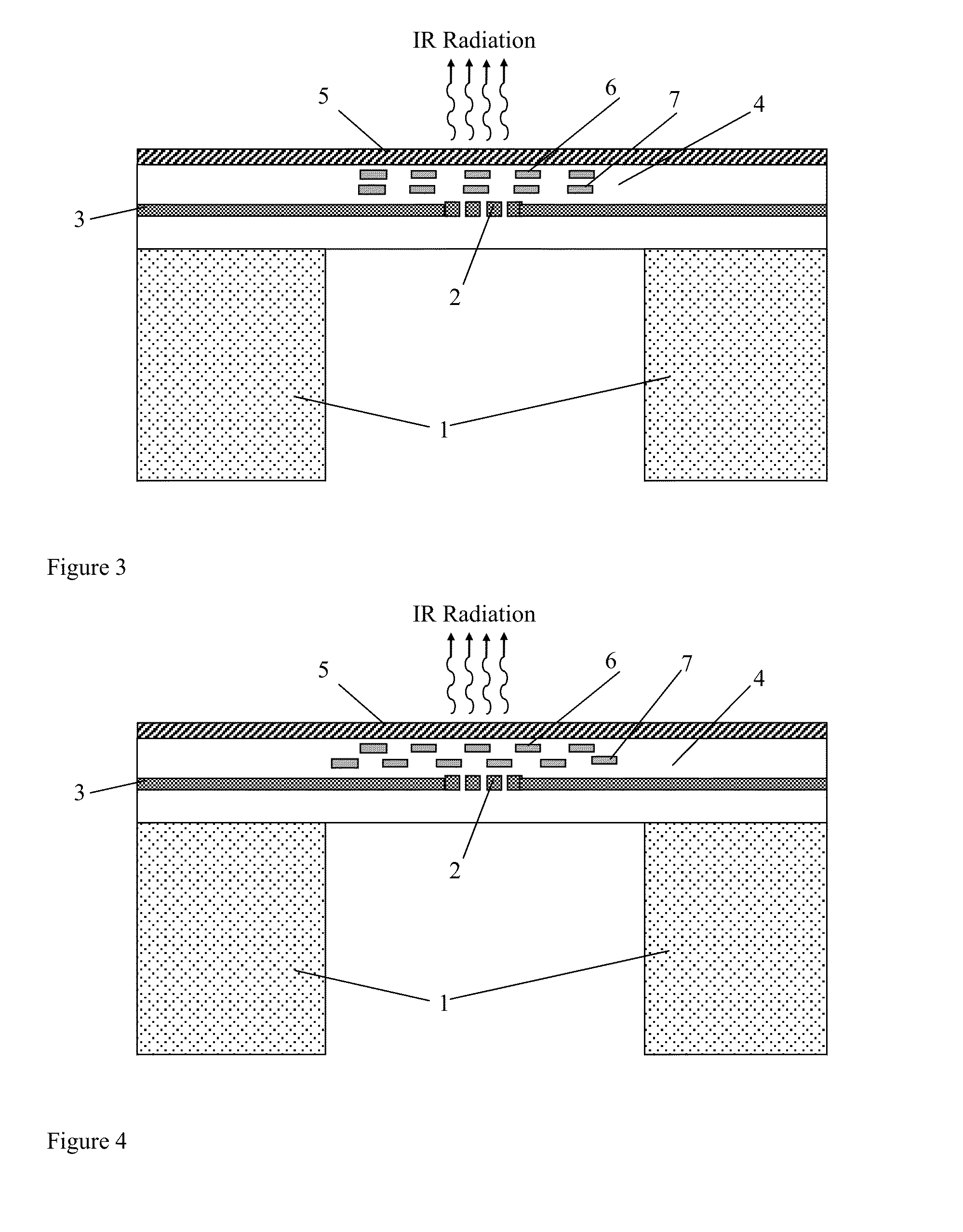
[0062]FIG. 1 shows a schematic cross section of an IR source with a plasmonic layer (or a patterned layer having laterally spaced structures) to enhance the IR emission. There is provided a membrane layer 4, 5 which is supported on a silicon substrate 1, the membrane layer including a dielectric layer 4 and a passivation layer 5. A tungsten resistive heater 2 is formed within the membrane 4, 5 and connected to the rest of a chip by tracks 3. The membrane includes a plasmonic layer 6 including a periodic pattern (or laterally spaced structures) and is located above the heater 2. The silicon substrate is etched by deep reactive ion etching (DRIE) which results in near vertical sidewalls. The heater 2 may be made from single crystal silicon, polysilicon, or a metal such as platinum, or a CMOS metal such as aluminium, tungsten, titanium, molybdenum or copper. The plasmonic layer has a periodic structure and may be made from polysilicon, a metal or a CMOS metal.

[0063]FIG. 2 shows a schem...


PUM


Abstract

An infra-red (IR) device comprising a dielectric membrane formed on a silicon substrate comprising an etched portion; and at least one patterned layer formed within or on the dielectric membrane for controlling IR emission or IR absorption of the IR device, wherein the at least one patterned layer comprises laterally spaced structures.

Description

RELATIONSHIP TO EARLIER APPLICATION[0001]This application is a continuation-in-part of U.S. application Ser. No. 13,466,626 filed on May 8, 2012 which is a continuation-in-part of U.S. application Ser. No. 12 / 691,104 filed on Jan. 21, 2010, hereby incorporated by reference in their entirety.FIELD OF THE INVENTION[0002]This invention relates to a thermal Infra-Red (IR) device using a micro-hotplate fabricated on a microchip and enhanced by the use of plasmonic structures. Particularly but not exclusively the invention relates to an IR source and an IR detector comprising plasmonic structures.BACKGROUND TO THE INVENTION[0003]It is well known to fabricate an IR Emitter based on silicon process. Such devices typically consist of a resistive micro-heater embedded within a thin membrane and supported on a silicon substrate. When current is passed through the heater, it heats up to a high temperature (which can be as much as 700° C. or even higher), and at this high temperature the device ...

Claims


Application Information

Patent Timeline
02 Oct 2014
Publication
US20140291704A1
IPC
H01L33/34; H01L33/00; H01L31/12; H01L31/18; H01L31/028; H01L27/15
CPC
H01L33/34; H01L31/028; H01L27/156; H01L31/12; H05B2214/04; H01L33/0054; H01L31/182; H05B3/267
Inventors
ALI, SYED ZEESHAN; UDREA, FLORIN