Method for coupling a graphene layer and a substrate and device comprising the graphene/substrate structure obtained

a graphene layer and substrate technology, applied in the field of coupling a graphene layer and a substrate, and a device comprising said graphene/substrat structure, can solve the problems of affecting the performance of the device, affecting the quality of the device, so as to hinder the implementation of high-temperature processes and reduce the quality

Active Publication Date: 2014-10-30
STMICROELECTRONICS INT NV
View PDF4 Cites 5 Cited by
  • Summary
  • Abstract
  • Description
  • Claims
  • Application Information

AI Technical Summary

Benefits of technology

[0045]This approach, which is rarely applied, presents the disadvantages typical of polymeric materials, namely, low temperature of vitreous transition, which hinders implementation of high-temperature processes, non-applicability on accentuated topography (>>10 nm), creation of a dielectric of lower quality than the insulators (gate oxide) most commonly used for producing an electronic device.

Problems solved by technology

Where the technique of production of graphene is based upon processes of CVD growth on metal substrates, or exfoliation techniques, in addition to the problem of choosing an adequate technique of transfer of the graphene onto a substrate, there is posed also the problem of identifying surface treatments capable of promoting adhesion of the graphene on the desired substrate, and at the same time, modulating appropriately the phenomena that occur at the graphene / insulator interface so that the electrical properties of the graphene will not be impaired by the treatment adopted.
The mechanical methods, generally based upon abrasion of the surface, are very rough and invasive.
These approaches, albeit modifying in a macroscopic way the surface (operating on the roughness, thickness, or planarity) frequently generate debris that abundantly contaminates the surface itself.
Silicon oxide (SiO2), the substrate that is commonly chosen for transfer and integration of the graphene, provides an excellent optical contrast, which, however, albeit enabling visual identification of the presence of the graphene, presents disadvantages linked to the surface roughness, to the high surface-charge concentration, to the presence of phonons, to the hydrophilic properties of the material, and to the low dielectric constant (κSiO2=3.9), which jeopardize the electrical performance thereof.
The graphene / silicon oxide interface is undoubtedly complex not only on account of the chemico-physical properties of silicon oxide, but also on account of the hydrophobic behavior of the graphene itself (the angle of contact measured on the graphene obtained by mechanical cleavage is 91°).
The poor adhesion of graphene on silicon oxide thus imposes a pre-treatment of the oxide for promoting adhesion and at the same time minimizing the chemico-physical interactions that jeopardize the electrical properties of the graphene.
In general, the most common wet treatment (SC-1) followed by oxygen plasma presents major limits of applicability.
Typically, it is used on a non-structured substrate of SiO2 and without metal contacts or interconnections, since the presence of solutions, such as H2O2 and the oxygen plasma itself, may dramatically jeopardize the pre-existing structure both from a morphological standpoint (roughness, wettability, phenomena of corrosion, chemical etching of the exposed surfaces, oxidation phenomena) and from an electrical standpoint (integrity of the metal surfaces, contact resistance).
However, this is an approach that cannot be applied over extensive areas (the size of the suspended graphene layer is tiny, just a few microns), it being markedly dependent upon the geometrical dimensions of the device.
This procedure presents the major limit of using dangerous chemical products, such as for example tetrahydrofuran, which reacts violently with oxidizing agents, generating explosions.
It is moreover highly flammable, and may give rise to phenomena of uncontrolled polymerization.
This approach, which is rarely applied, presents the disadvantages typical of polymeric materials, namely, low temperature of vitreous transition, which hinders implementation of high-temperature processes, non-applicability on accentuated topography (>>10 nm), creation of a dielectric of lower quality than the insulators (gate oxide) most commonly used for producing an electronic device.

Method used


Image

  • Method for coupling a graphene layer and a substrate and device comprising the graphene/substrate structure obtained
  • Method for coupling a graphene layer and a substrate and device comprising the graphene/substrate structure obtained
  • Method for coupling a graphene layer and a substrate and device comprising the graphene/substrate structure obtained

Examples


Embodiment Construction

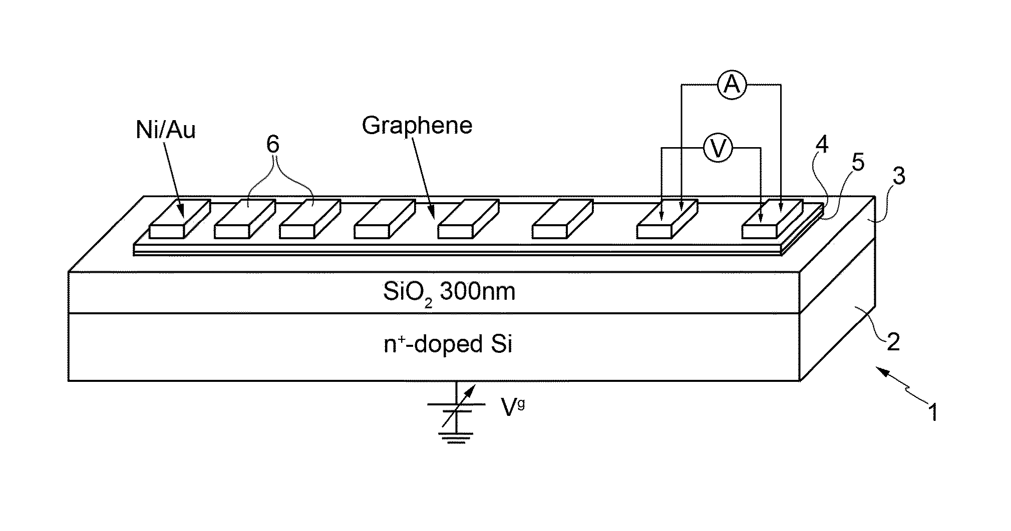
[0061]One or more embodiments of the present disclosure regards a method for coupling a graphene layer 4 to a substrate 2 having at least one hydrophilic surface 3, the method comprising the steps of:[0062]providing a substrate 2 having at least one hydrophilic surface 3;[0063]depositing on the hydrophilic surface 3 a layer of a solvent 5 selected in the group constituted by acetone, ethyl lactate, isopropyl alcohol, methylethyl ketone and mixtures thereof; and[0064]depositing on the solvent layer 5 a graphene layer 4.

[0065]According to one embodiment, the hydrophilic surface 3 is made of silicon oxide.

[0066]The substrate 2 is preferably made of silicon oxide or passivized silicon. According to one embodiment the solvent may be a mixture of methylethyl ketone and ethyl lactate preferably present in a percentage of 40% and 60%, respectively.

[0067]Deposition of the solvent layer 5 may be obtained via dipping of the substrate in the solvent or via spin-coating.

[0068]In one embodiment, ...


PUM


Abstract

The present disclosure regards a method for coupling a graphene layer to a substrate having at least one hydrophilic surface, the method comprising the steps of providing the substrate having at least one hydrophilic surface, depositing on the hydrophilic surface a layer of a solvent selected in the group constituted by acetone, ethyl lactate, isopropyl alcohol, methylethyl ketone and mixtures thereof and depositing on the solvent layer a graphene layer. It moreover regards an electronic device comprising the graphene/substrate structure obtained.

Description

BACKGROUND[0001]1. Technical Field[0002]The present disclosure relates to a method for coupling a graphene layer and a substrate, and a device comprising said graphene / substrate structure.[0003]2. Description of the Related Art[0004]In the last few years, application of surface-treatment techniques has made it possible to improve the properties of materials, involving an extremely wide range of industrial sectors, from the mechanical sector to the biomedical sector. The development of such treatments is the result of a considerable progress in research, pushed by the desire to increase the performance and potentialities of the surfaces treated and by the desire to reduce costs.[0005]Application of such treatments, associated to the study of the interfaces of the materials involved, is fundamental in the development of systems that present a high surface / volume ratio since the phenomena that occur at the interface affect the physics of the system under examination, all the more, the ...

Claims


Application Information

Patent Timeline
Patent Type & Authority Applications(United States)
IPC IPC(8): H01L21/02H01L29/16
CPCH01L29/1606H01L21/02376H01L21/7624G01R31/2648H01L29/66742H01L29/78603H01L29/78684H01L31/028
Inventor SPARTA', NOEMI GRAZIANATRINGALI, CRISTINALOVERSO, STELLARAVESI, SEBASTIANOACCARDI, CORRADOGIANNAZZO, FILIPPO
Owner STMICROELECTRONICS INT NV
Why Eureka
Try Eureka