Organic Electronic Device

a technology of electronic devices and thin films, applied in thermoelectric devices, organic chemistry, group 5/15 element organic compounds, etc., can solve the problems of high operating voltage, difficult processing, and high reactiveness of thin film transistors, and achieve the effect of lowering operating voltage, improving oled life, and improving electronic interface to cathod

Active Publication Date: 2014-12-04
NOVALED GMBH
View PDF1 Cites 15 Cited by
  • Summary
  • Abstract
  • Description
  • Claims
  • Application Information

AI Technical Summary

Benefits of technology

[0061]Surprisingly, it was observed an improvement of the OLED lifetime, and a lowering of the operating voltage.
[0062]Polymer Hybrid OLED or Solar Cell
[0063]In a further preferred embodiment the substantially organic layer comprising the chemical compound according to formula (I) is used in combination with a polymer semiconductor, preferably between a cathode and a polymer layer, wherein the polymer layer preferably comprises the optoelectronic active region of the device (emitting region of an OLED or the absorbing region of a solar cell). All alternatives of layers comprising the chemical compound according to formula (I) or being composed thereof can be used in combination with that polymer layer. Exemplary alternative layers can be an injection layer being composed of the chemical compound according to formula (I), an injection layer comprising the chemical compound and a metal, an electron transport layer having the chemical compound with or without a metal. The electronic interface to the cathode is then strongly improved given the high electron injection capability of the chemical compound (I).
[0064]The invention can be used as an alternative to conventional doping of organic semiconducting layers. By using the term doping it is meant electrical doping as explained above. This doping can also be called redox-doping or charge transfer doping. It is known that the doping increases the density of charge carriers of a semiconducting matrix towards the charge carrier density of the undoped matrix. An electrically doped semiconductor layer also has an increased effective mobility in comparison with the undoped semiconductor matrix.
[0065]US2008227979 discloses in detail the doping of organic transport materials, also called ma-trix, with inorganic and with organic dopants. Basically, an effective electronic transfer occurs from the dopant to the matrix increasing the Fermi level of the matrix. For an efficient trans-fer in a p-doping case, the LUMO energy level of the dopant is preferably more negative than the HOMO energy level of the matrix or at least slightly more positive, not more than 0.5 eV, to the HOMO energy level of the matrix. For the n-doping case, the HOMO energy level of the dopant is preferably more positive than the LUMO energy level of the matrix or at least slightly more negative, not lower than 0.5 eV, to the LUMO energy level of the matrix. It is further more desired that the energy level difference for energy transfer from dopant to matrix is smaller than +0.3 eV.
[0066]Typical examples of doped hole transport materials are: copperphthalocyanine (CuPc), which HOMO level is approximately −5.2 eV, doped with tetrafluoro-tetracyanoquinonedimethane (F4TCNQ), which LUMO level is about −5.2 eV; zincphthalocyanine (ZnPc) (HOMO=−5.2 eV) doped with F4TCNQ; a-NPD (N,N′-Bis(naphthalen-1-yl)-N,N-bis(phenyl)-benzidine) doped with F4TCNQ.

Problems solved by technology

However, convention organic thin film transistors (OTFTs) require very high voltages to operate.
However, these materials are highly reactive, difficult to process and are only suitable to a limited extent as electrode materials.
Moreover, any reduction in operating voltage brought about by using such cathodes is only partial.
However, the use of low work function metals has several disadvantages.
It is well known that the metals can easily diffuse through the semiconductor, eventually arriving at the optically active layer quenching the excitons, thereby lowering the efficiency of the device and the lifetime.
Another disadvantage is their high susceptibility to oxidation upon exposure to air.
Therefore, devices using such metals as dopants, injection or cathode material require rigorous exclusion of air during production and rigorous encapsulation afterwards.
Another well known disadvantage is that higher molar doping concentration of the dopant exceeding 10 mol.
Yet another problem is high volatility of many simple redox dopants like Cs, leading to cross-contamination in the device assembling process making their use in device fabrication tools less attractive.
Due to their still high enough electron donating capability, they are also undergoing rapid decay upon exposure to air, making their handling in device production difficult.
Investigations have shown that the use of LiQ still leads to OLEDs with high operating voltage.

Method used


Image

  • Organic Electronic Device
  • Organic Electronic Device
  • Organic Electronic Device

Examples


##ventive example 1

Inventive Example 1

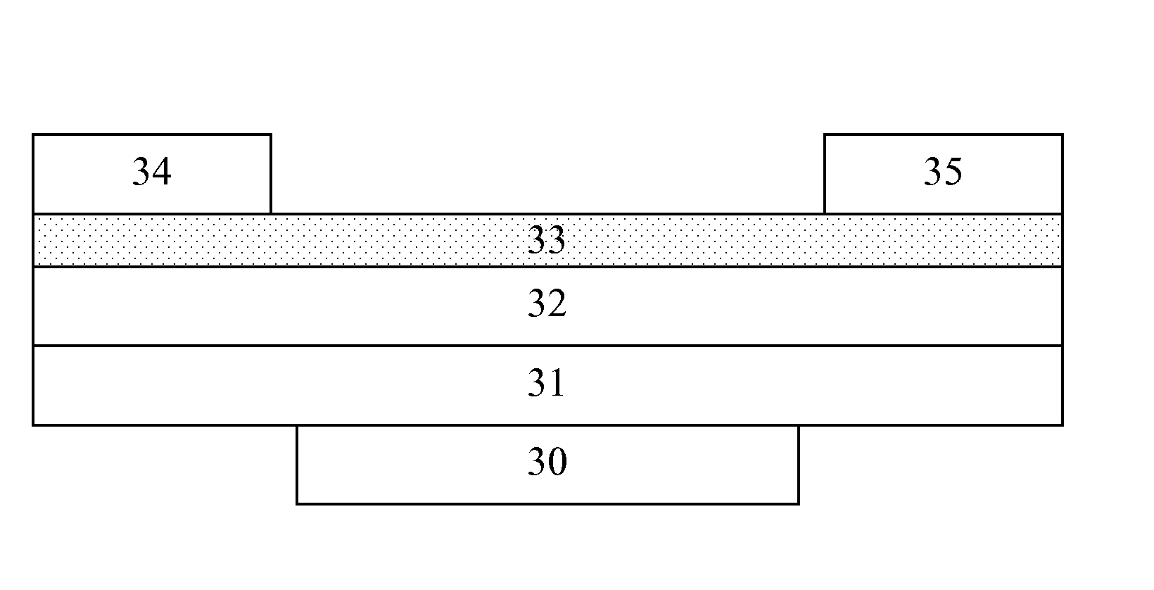
[0128]A similar device was produced as in Comparative Example 1, with the difference that the ETL was deposited as a 36 nm thick layer of a mixture between the compound according to Formula (I) and ETM1 with a weight ratio of 1:1.

[0129]This device showed a slightly increased voltage of 4.3 V at a current density of 10 mA / cm2, an extremely enhanced luminance of 532 cd / m2 at a current density of 10 mA / cm2 with a current efficiency of 5.3 cd / A at the same current density. These values are remarkable good for a blue emitting OLED. Given the high performance, it is possible to operate an OLED with same or higher light intensity than the OLEDs of the comparative examples at a lower voltage.

[0130]OLEDs with other ETMs and the compound according to Formula (I) showed similar performance improvements OLEDs with other ETMs and the compound according to Formula (I) showed similar performance improvements, as shows the Table 1:

ETL Voltage (V) CIE CIE QEff (%) atcompoundmatrix...


PUM


Abstract

The present invention relates to an organic electronic device, comprising a first electrode, a second electrode, and a substantially organic layer comprising a compound according to formula (I) between the first and the second electrode:
wherein A1 is a C6-C20 arylene and each of A2-A3 is independently selected from a C6-C20 aryl, wherein the aryl or arylene may be unsubstituted or substituted with groups comprising C and H or with a further LiO group, provided that the given C count in an aryl or arylene group includes also all substituents present on the said group.

Description

FIELD OF THE INVENTION[0001]The present invention relates to an organic electronic device and to a use of a specific compound in such an organic electronic device.BACKGROUND[0002]Organic electronic devices, such as organic semiconductors, can be used to fabricate simple electronic components, e.g. resistors, diodes, field effect transistors, and also optoelectronic components like organic light emitting devices (e.g. organic light emitting diodes (OLED)), and many others. The industrial and economical significance of the organic semiconductors and their devices is reflected in the increased number of devices using organic semiconducting active layers and the increasing industry focus on the subject.[0003]OLEDs are based on the principle of electroluminescence in which electron-hole pairs, so-called excitons, recombine under the emission of light. To this end the OLED is constructed in the form of a sandwich structure wherein at least one organic film is arranged as active material b...

Claims


Application Information

Patent Timeline
Patent Type & Authority Applications(United States)
IPC IPC(8): H01L51/00H01L51/44H01L51/52H01L51/05
CPCH01L51/0062H01L51/0512H01L51/5092H01L51/52H01L51/5072H01L51/44C07F9/5325C07F9/5765C09K11/06C09K2211/181H10K85/60H10K85/30H10K85/6572H10K50/171H10K50/16Y02E10/549H10K10/462H10K50/80H10K85/649H10K30/80
Inventor DOROK, SASCHAROTHE, CARSTENFADHEL, OMRANECARDINALI, FRANCOIS
Owner NOVALED GMBH
Why Eureka
Try Eureka