Lateral power semiconductor transistors

a technology of semiconductor transistors and transistors, applied in semiconductor devices, diodes, electrical devices, etc., can solve the problems of increasing switching losses, reducing on-state losses, and devices with high current capability, and achieves higher doping concentration and high doping concentration

Active Publication Date: 2015-01-08
CAMBRIDGE MICROELECTRONICS LTD
View PDF5 Cites 20 Cited by
  • Summary
  • Abstract
  • Description
  • Claims
  • Application Information

AI Technical Summary

Benefits of technology

[0018]According to one aspect of the present invention there is provided a lateral bipolar power semiconductor transistor comprising: a contact region of a first conductivity type located within a first semiconductor region of a second, opposite conductivity type; a source region of the second conductivity type located within a second semiconductor region of the first conductivity type; a lateral drift region of the second conductivity type placed between the first semiconductor region and the second semiconductor region, the lateral drift region to be depleted of mobile carriers at breakdown voltage during an off-state blocking mode of the transistor and able to conduct charge during an on-state conducting mode of the transistor; a gate placed above and in direct contact to the second semiconductor region, the gate to control ch...

Problems solved by technology

In power ICs, such devices are often monolithically integrated with CMOS-type or BiCMOS-type low voltage/low power circuits.
However, in general, a high level of charge leads to reduced on-state losses but increased switching losses.
The vertical devices have high current capability, but they are not CMOS compatible.
Lifetime killing in lateral power devices can be challenging since it can damage the CMOS or Bi-CMOS circuit blocks in an integrated circuit.
Changing the doping of the layers can be very difficult for lateral power devices, because most layers available in a CMOS or bi-CMOS process have doping concentrations dictated by the performance of the CMOS or Bi-CMOS low voltage devices.
The process therefore has to be re-tailored to allow this change, which can...

Method used


Image

  • Lateral power semiconductor transistors
  • Lateral power semiconductor transistors
  • Lateral power semiconductor transistors

Examples


Embodiment Construction

[0053]The following describes arrangements falling within the broader aspects of the present invention summarised above, and more specific embodiments.

[0054]Embodiments are particularly concerned with high voltage semiconductor devices which can be used in power integrated circuits and have particular application to MOS-bipolar transistors.

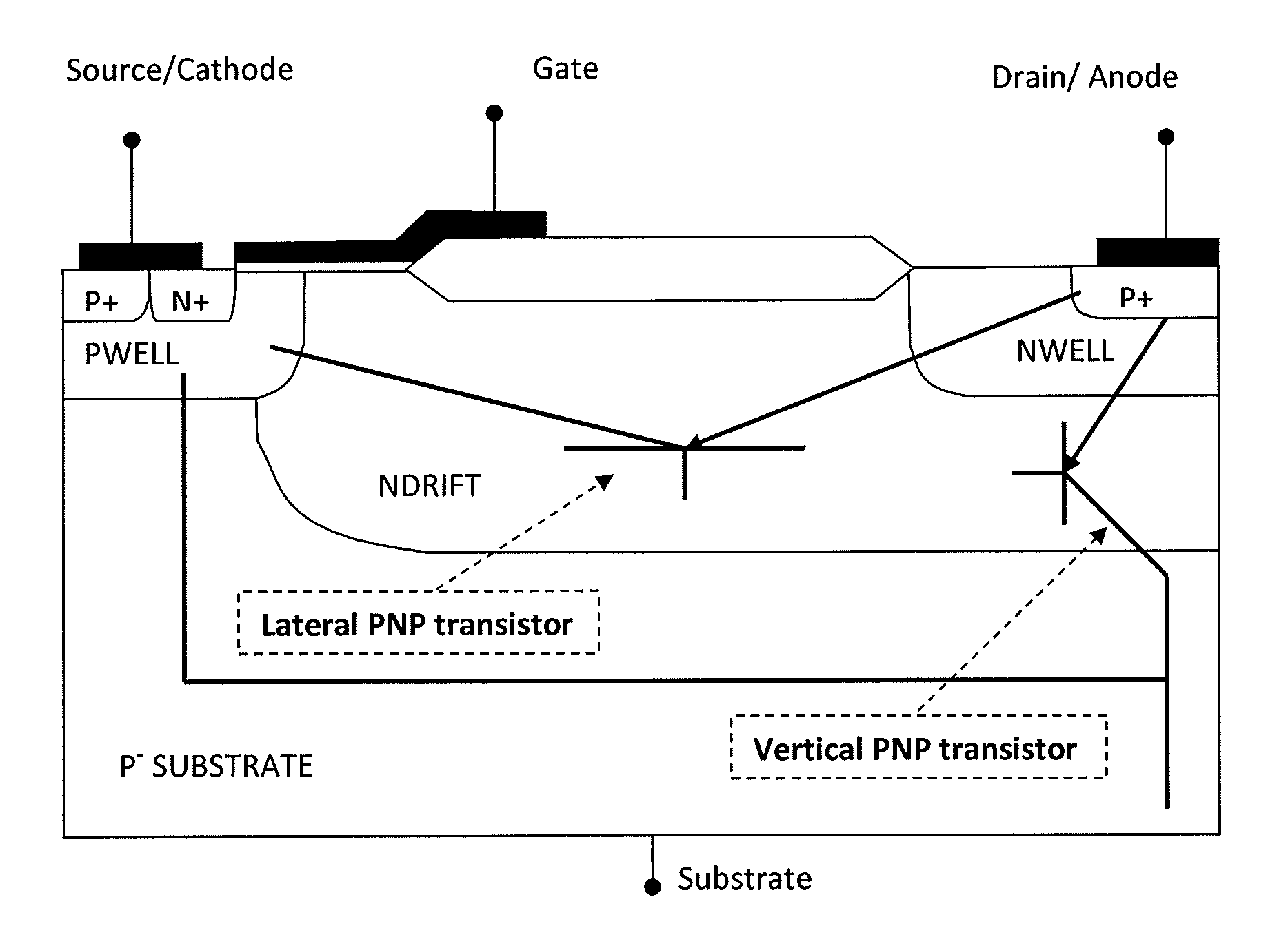
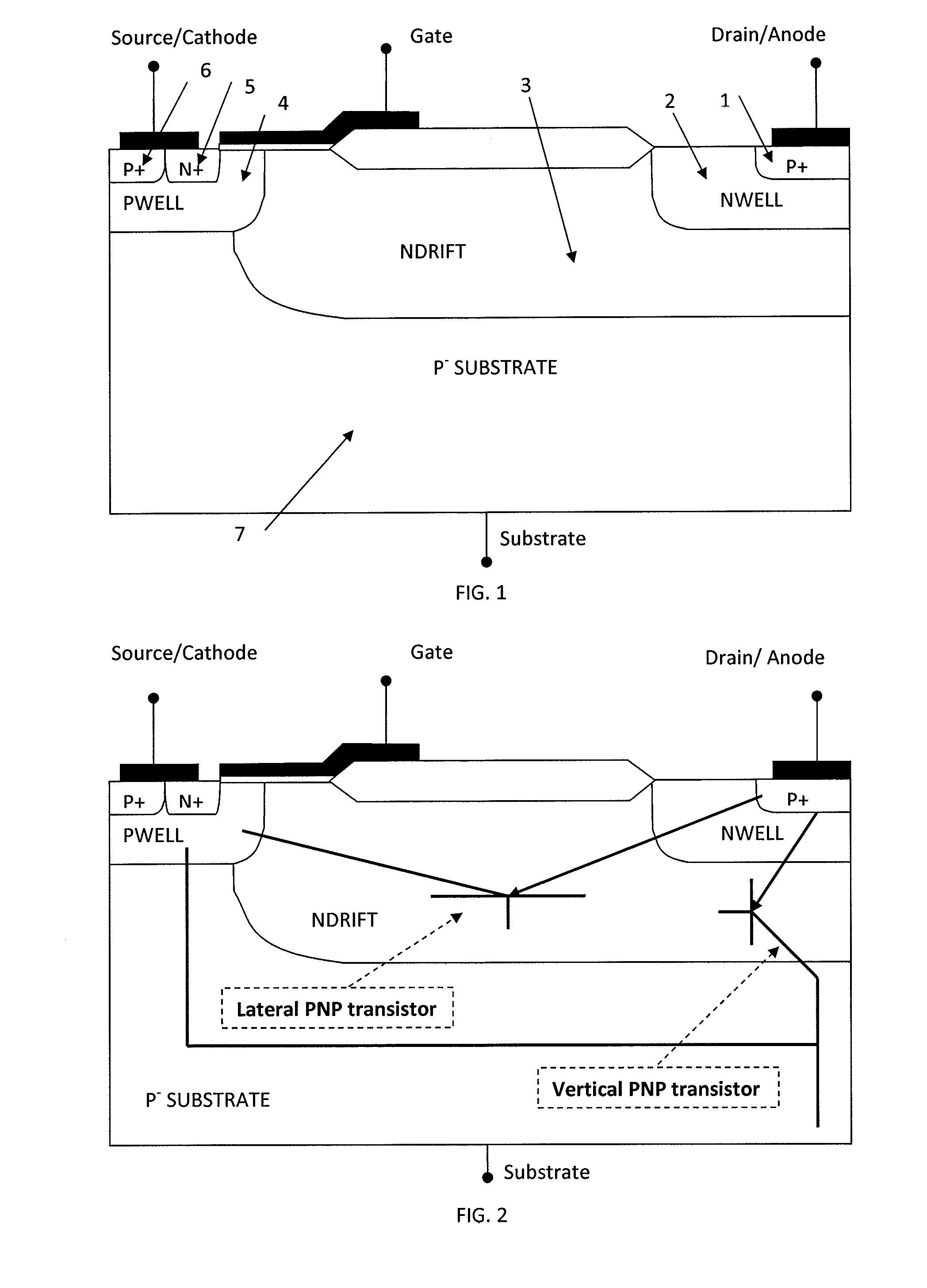
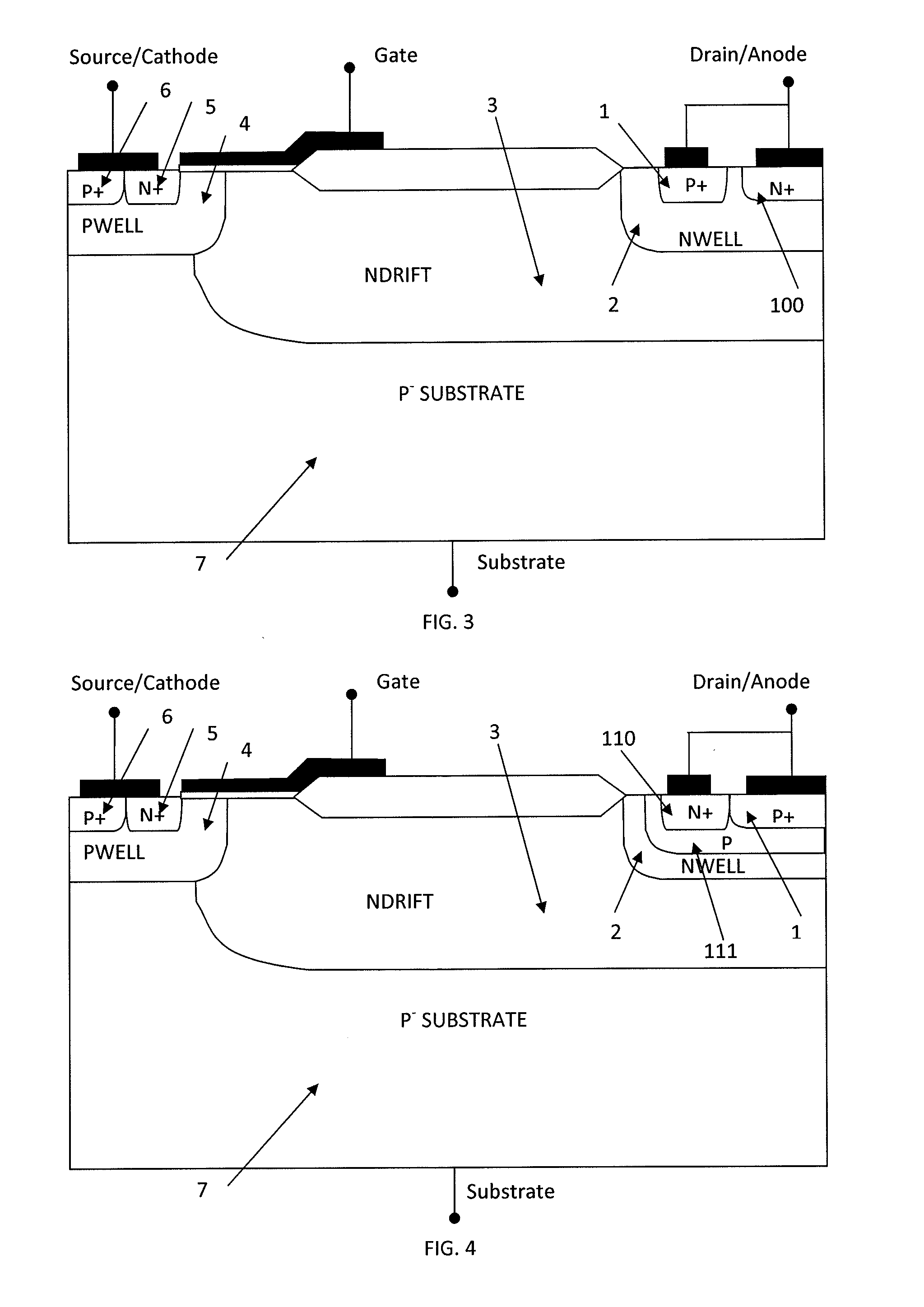
[0055]FIG. 5 shows the cross sectional view of a LIGBT according to one embodiment of the invention. In this embodiment, the LIGBT includes a substrate region 7 having high resistivity; a drift layer 3 formed in the substrate region 7 and resistivity of this layer 3 dependent on the off state blocking voltage of the LIGBT. The LIGBT further includes a p-well layer 4 formed at the common surface of the drift layer 3 and substrate 7; a source layer 5 formed at the surface of the p-well layer 4; a body layer 6 formed at the surface of the p-well layer 4; and a source electrode which is ohmic is arranged in contact with the source and body layers 5, 6...


PUM


Abstract

The invention generally relates to a lateral power semiconductor transistor for example in integrated circuits. In particular the invention relates to Lateral Insulated Gate Bipolar Transistors or other lateral bipolar devices such as PIN diodes. The invention also generally relates to a method of increasing switching speed of a lateral bipolar power semiconductor transistor. There is provided a lateral bipolar power semiconductor transistor comprising a first floating semiconductor region of the first conductivity type located laterally spaced to an anode/drain region and a second floating semiconductor region of the second conductivity type located laterally adjacent the first floating semiconductor region, and a floating electrode placed above and in direct contact to the first and second floating semiconductor regions.

Description

FIELD OF THE INVENTION[0001]The invention generally relates to a lateral power semiconductor transistor, particularly but not exclusively to a lateral insulated gate bipolar transistor (LIGBT). The invention also generally relates to a method of increasing switching speed of a lateral bipolar power semiconductor transistor.BACKGROUND TO THE INVENTION[0002]A power semiconductor device is a semiconductor device used as a switch or rectifier in power electronics (e.g. switch-mode power supply). Such a device could be used in an integrated circuit, and the circuit becomes a Power IC, a High Voltage IC or a Smart Power circuit. A power semiconductor device is usually used in “commutation mode” (i.e. it is either on or off), and therefore has a design optimized for such usage.[0003]High power devices used in integrated circuits typically operate with voltages in the range of 20V to 1.2 kV and current levels in the range of 1 mA to 50 A. Their application areas range from portable consumer...

Claims


Application Information

Patent Timeline
IPC IPC(8): H01L29/739H01L27/06H01L29/66
CPCH01L29/7393H01L27/067H01L29/66325H01L29/0834H01L29/7398H01L29/423H01L29/7394
Inventor PATHIRANA, VASANTHAUDUGAMPOLA, NISHADTRAJKOVIC, TANYA
Owner CAMBRIDGE MICROELECTRONICS LTD
Why Eureka
Try Eureka