
System for performing laser filamentation within transparent materials

a technology of transparent materials and lasers, applied in glass making apparatus, manufacturing tools, welding/soldering/cutting articles, etc., can solve the problems of increased production cost, increased cleaning and polishing steps, and poor quality edges, so as to facilitate active control of the process and facilitate the formation of filament arrays

Inactive Publication Date: 2015-02-05
ROFIN SINAR TECH
View PDF14 Cites 57 Cited by
  • Summary
  • Abstract
  • Description
  • Claims
  • Application Information

AI Technical Summary

Benefits of technology

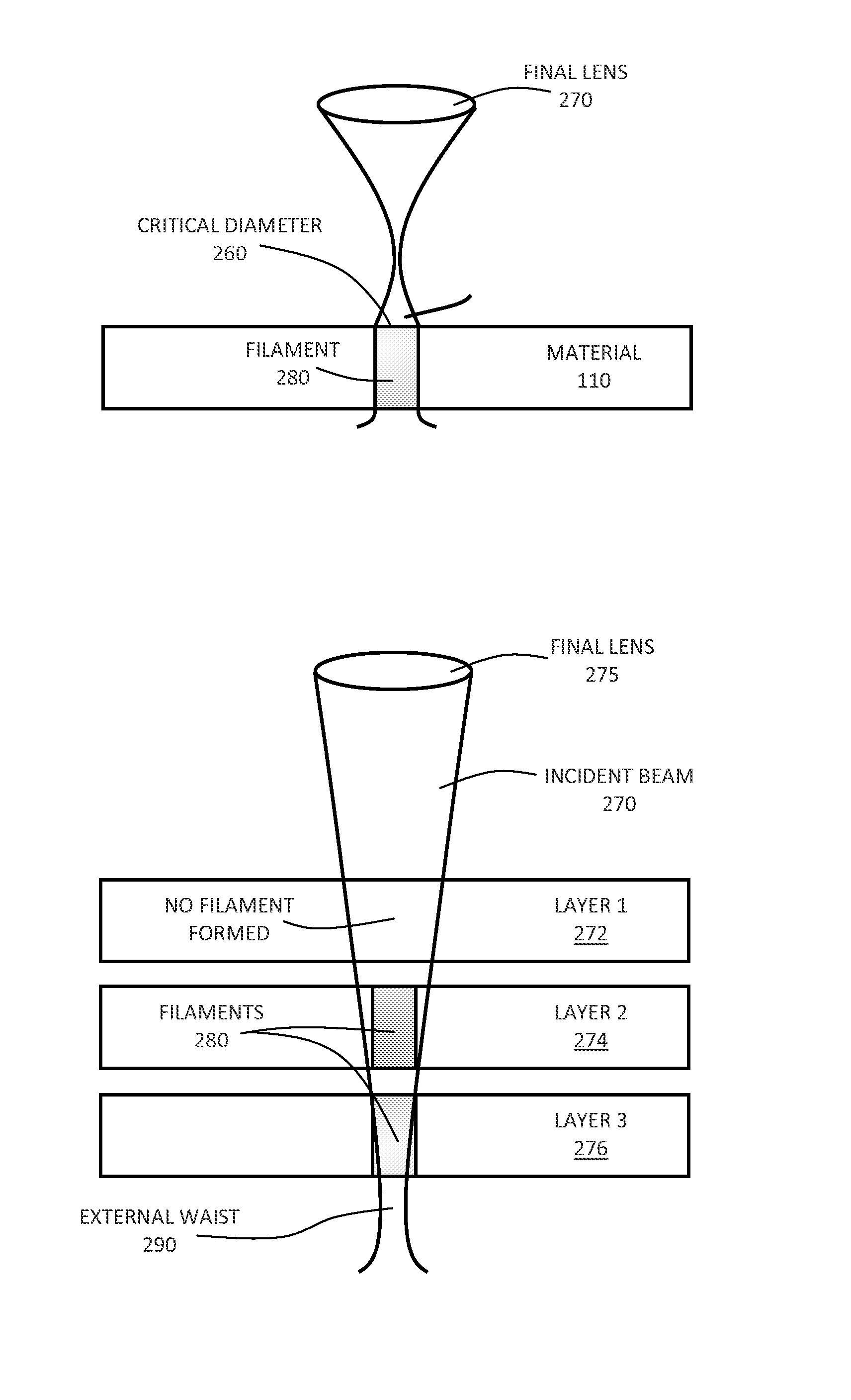
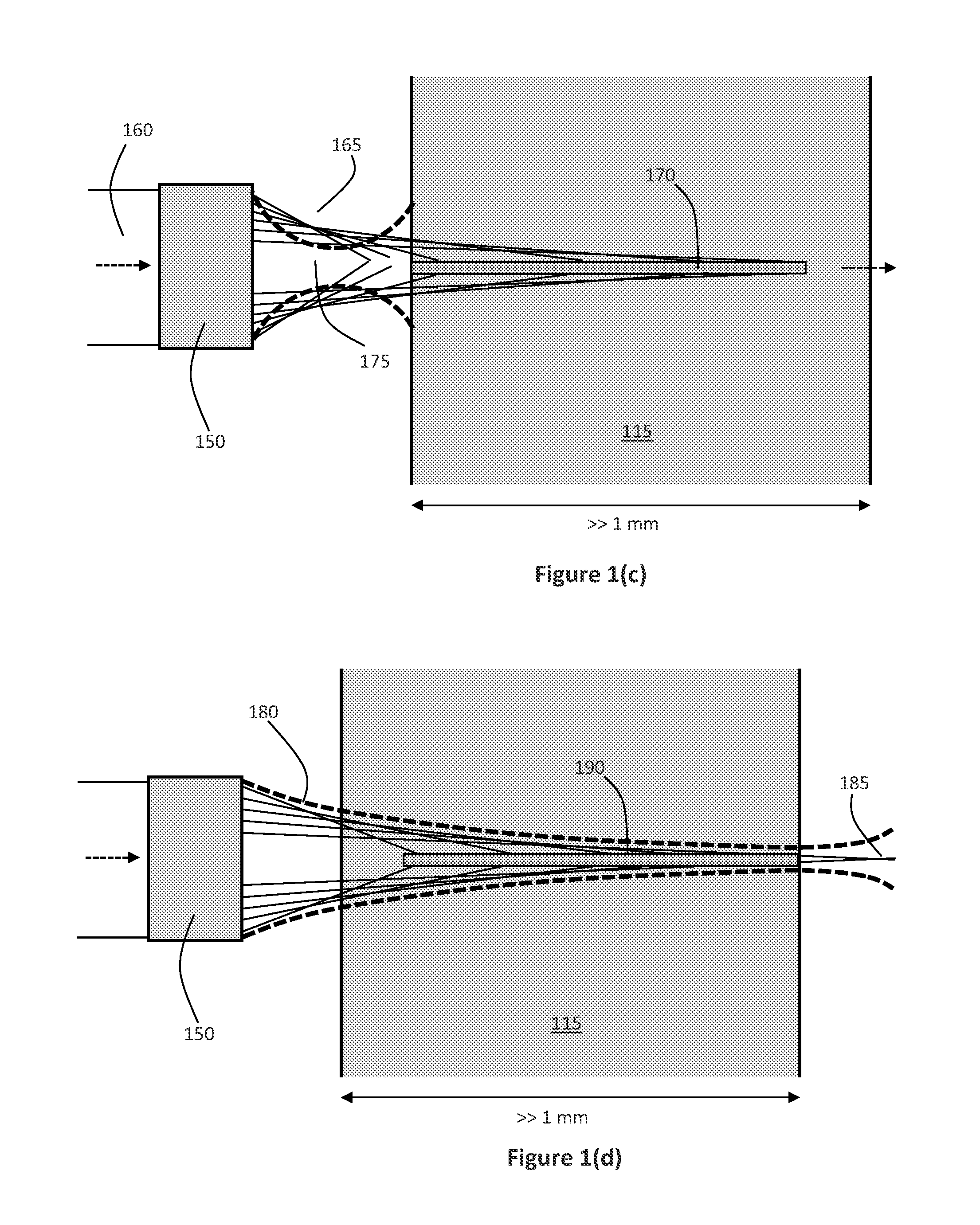
The patent describes a system and method for creating continuous laser filments in transparent materials. The system uses a burst of ultrafast laser pulses that are focused outside of the material to prevent damage. The laser pulses create a high energy density in the material that supports the formation of a continuous filament without causing optical breakdown. The resulting filaments are long and have a taper-free profile. The system can also be used to create filament arrays for cleaving and marking. The process can be monitored and controlled optically. The patent also describes a method for creating ablative markings in a metal layer by using a low-power laser beam. The system includes one or more focusing elements to external focus the laser beam and create a continuous laser filament without damaging the material.

Problems solved by technology

This process creates poor quality edges, microcracks, wide kerf width, and substantial debris that are major disadvantages in the lifetime, efficiency, quality, and reliability of the product, while also incurring additional cleaning and polishing steps.
The cost of de-ionized water to run the diamond scribers are more than the cost of ownership of the scriber and the technique is not environmentally friendly since water gets contaminated and needs refining, which further adds to the production cost.
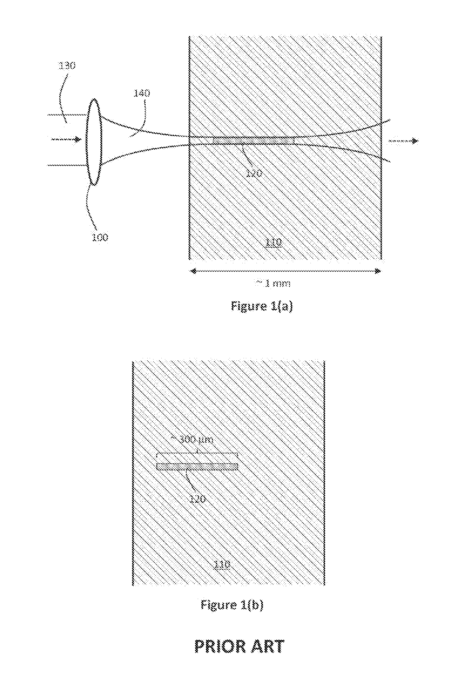
Unfortunately, known laser processing methods have disadvantages, particularly in transparent materials, such as slow processing speed, generation of cracks, contamination by ablation debris, and moderated sized kerf width.
Furthermore, thermal transport during the laser interaction can lead to large regions of collateral thermal damage (i.e. heat affected zone).
However, the aforementioned disadvantages cannot be eliminated due to the aggressive interactions inherent in this physical ablation process.
This is amply demonstrated by the failings of UV processing in certain LED applications where damage has driven the industry to focus on traditional scribe and break followed by etch to remove the damaged zones left over from the ablative scribe or the diamond scribe tool, depending upon the particular work-around technology employed.
However, in general, the machining of transparent materials with pulses even as short as tens to hundreds of femtosecond is also associated with the formation of rough surfaces, slow throughput and micro-cracks in the vicinity of laser-formed kerf, hole or trench that is especially problematic for brittle materials like alumina (Al2O3), glasses, doped dielectrics and optical crystals.
Further, ablation debris will contaminate the nearby sample and surrounding devices and surfaces.
This approach suffers from the need to make multiple passes and therefore results in low processing throughput.
Although laser processing has been successful in overcoming many of the limitations associated with diamond cutting, as mentioned above, new material compositions have rendered the wafers and panels incapable of being laser scribed.
Furthermore, the size of the devices and dice on the wafers are getting smaller and closer to each other that limit the utility of both diamond and conventional laser-based scribing.
For example, 30 μm is a feasible scribing width, while 15 μm is challenging for these conventional methods.
Moreover, as diamond scribing uses mechanical force to scribe the substrate, thin samples are very difficult to scribe.
Due to the use of increasingly exotic and complex material stacks in the fabrication of wafer-based devices, the laser scribing techniques previously applied will simply no longer work due to the opacity of the stack.

Method used


Image

  • System for performing laser filamentation within transparent materials
  • System for performing laser filamentation within transparent materials
  • System for performing laser filamentation within transparent materials

Examples


example 1

Singulation of Glass Samples Via Laser Filamentation

[0244]To demonstrate some of the embodiments disclosed above, glass samples were processed on a laser system equipped with a 50W ps laser operating at high rep rate (>400 kHz) to facilitate very rapid scans of the laser beam across the target, with stages moving at a rate of approximately 500 mm / s—1000 mm / s, where 0.7 mm thick Gorilla glass had been mounted. The laser, operating at the fundamental, 1064 nm with a pulse width less than 25 ps, was set to operate in burst mode with 20 sub-pulses in a burst.

[0245]Both rectilinear cuts and curvilinear shapes have been achieved at high speed with very good edge quality and high bend strength. For example, samples of Gorilla thus processed have shown >110 MPa as-cut bend strength. FIG. 19 shows a micrograph of the facet edge after formation of the modified zone (the so-called scribe step) and the cleave step (singulation). The roughness shown is less than 10 μm RMS over a substantial port...

example 2

Formation of 6 mm Long Filaments in Glass Substrates

[0255]In one example implementation, the laser beam may include a burst of pulses having a pulse duration less than approximately 500 ps, which is collimated and focused to a spot outside of the target (for example, with a waist greater than approximately 1 μm and less than approximately 100 μm. Without intending to be limited by theory, and as noted above, it is believed that the non-linear interactions that result in filament formation cause a series of acoustic compressions within the material. These acoustic compressions are understood to be substantially symmetric about the beam axis. The longitudinal length of this zone is determined by a number of pulse and beam parameters, including the position of the focus, the laser power and the pulse energy, as described above.

[0256]For example, using a 50W laser with a burst train of pulses each having a pulsewidth of approximately 10 ps, with a 2 MHz rep rate, for example, filaments ...

example 3

Filament Formation Using 1064 nm Pulsed Laser

[0259]In one example implementation of the methods, apparatus and systems disclosed herein, a laser configured to output bursts of picosecond pulses as described is admitted to an optical train with a collimator and steering optics, optionally a scanner with a field corrected region capable of delivering at user selectable angles, a beam with optics designed to induce aberrated wavefronts which can be focused via negative or positive lenses such that the interaction zone exceeds the depth of the target layer to be scribed. In one example implementation, bursts of picosecond pulses emitted at 5 MHz from a 50W 1064 nm laser is focused by a series of lenses to create a 5 μm spot at focus outside the material using a doublet or triplet of lenses where the ratio, W, of focal lengths lies between −20 and +20 (L1fl / L2fl=W), depending upon the target substrate and the intended final result (full cut, scribe and break, etc.) as the length of the i...


PUM

PropertyMeasurementUnit
Lengthaaaaaaaaaa
Temperatureaaaaaaaaaa
Timeaaaaaaaaaa

Abstract

Systems and methods are described for forming continuous laser filaments in transparent materials. A burst of ultrafast laser pulses is focused such that a beam waist is formed external to the material being processed without forming an external plasma channel, while a sufficient energy density is formed within an extended region within the material to support the formation of a continuous filament, without causing optical breakdown within the material. Filaments formed according to this method may exhibit lengths exceeding up to 10 mm. In some embodiments, an aberrated optical focusing element is employed to produce an external beam waist while producing distributed focusing of the incident beam within the material. Various systems are described that facilitate the formation of filament arrays within transparent substrates for cleaving / singulation and / or marking. Optical monitoring of the filaments may be employed to provide feedback to facilitate active control of the process.

Description

[0001]This patent application claims priority to and the benefit of United States provisional patent application Ser. No. 61,861,880 filed Aug. 2, 2013. United States provisional patent application Ser. No. 61,861,880 filed Aug. 2, 2013 is incorporated herein in its entirety by reference hereto.FIELD OF THE INVENTION[0002]The invention is in the field of laser filamentation within transparent materials.BACKGROUND OF THE INVENTION[0003]The present disclosure is related to systems and methods for the laser processing of materials. More particularly, the present disclosure is related to systems and methods for the singulation and / or cleaving of wafers, substrates, and plates containing passive or active electronic or electrical devices created upon said materials.[0004]In current manufacturing, the singulation, dicing, scribing, cleaving, cutting, and facet treatment of wafers or glass panels is a critical processing step that typically relies on diamond or conventional, ablative or br...

Claims


Application Information

Patent Timeline
IPC IPC(8): B23K26/30
CPCB23K26/426B23K26/53B23K26/0648B23K26/38C03B33/0222C03B33/07C03B33/04C03B33/033B23K2103/00B23K26/0006B23K26/082B23K26/0624B23K2103/54B23K2103/42B23K2103/50B23K2103/52B23K2103/56H01L21/78B23K26/083B23K26/064B23K26/04B23K26/0626C03C14/002C03C2214/02C03B33/09
Inventor HOSSEINI, S. ABBAS
Owner ROFIN SINAR TECH
Learn More