Type of fine metal mask (FFM) used in OLED production and the method of manufacturing it
- Summary
- Abstract
- Description
- Claims
- Application Information
AI Technical Summary
Benefits of technology
Problems solved by technology
Method used
Image
Examples
first embodiment
The First Embodiment
[0030]First embodiment of manufacturing an fine metal mask used in OLED production includes the following steps:
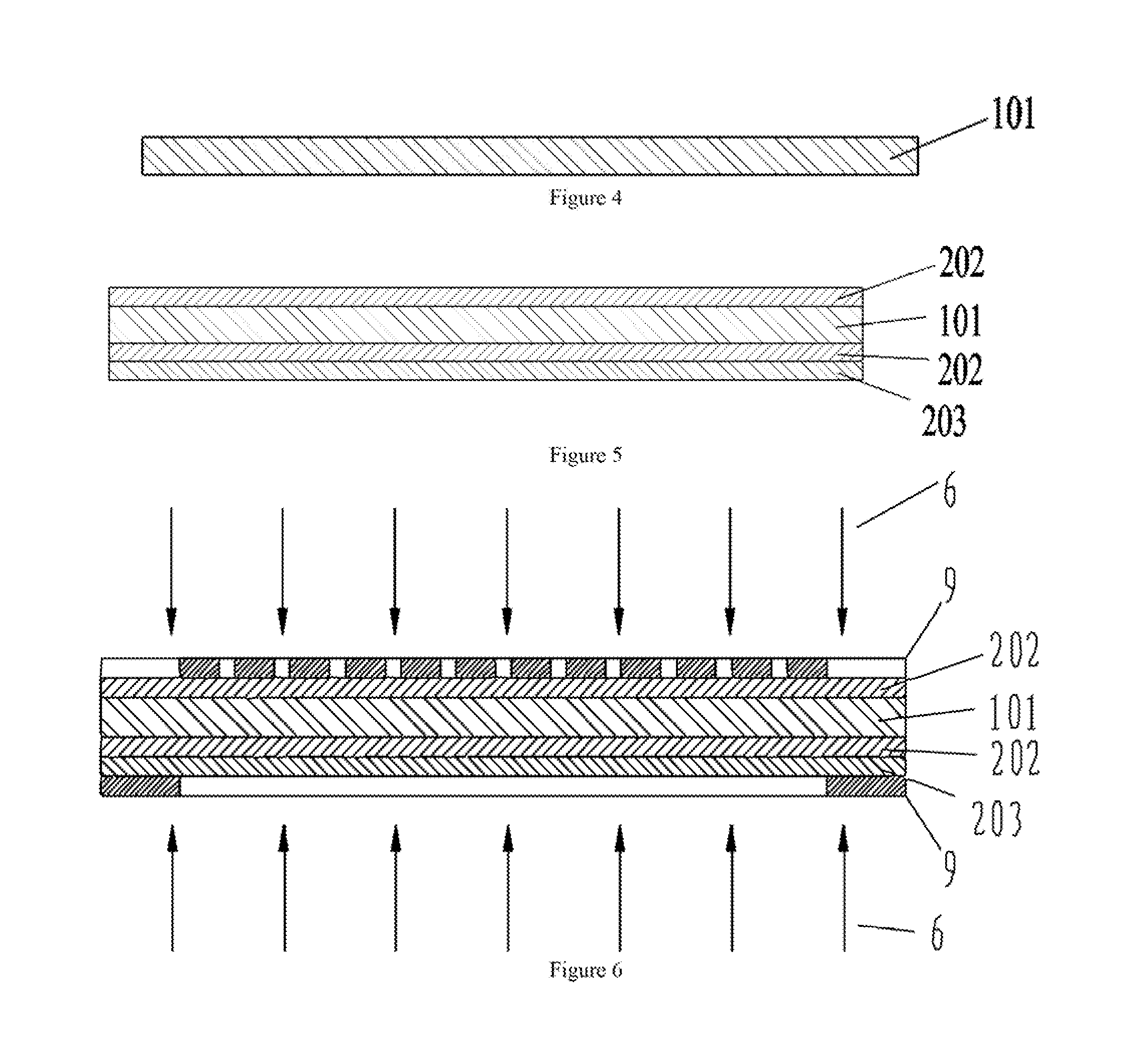
[0031]1. Clean a 1 mm±5 μm invar steel substrate (101) by acid, organic solvent and deionized water ultrasonic for about 5-15 min, and then dry the substrate in clean drying box.
[0032]2. Coat both sides of the invar steel substrate (101) with a 55 μm photoresist layer (202), and the bottom photoresist layer (202) with a layer of photoresist protective film (203).
[0033]3. Expose the top and bottom photoresist layers (202) at the same time by the parallel light from a laser direct image exposure machine wherein the pattern that needs to be exposed has been imported into computer.
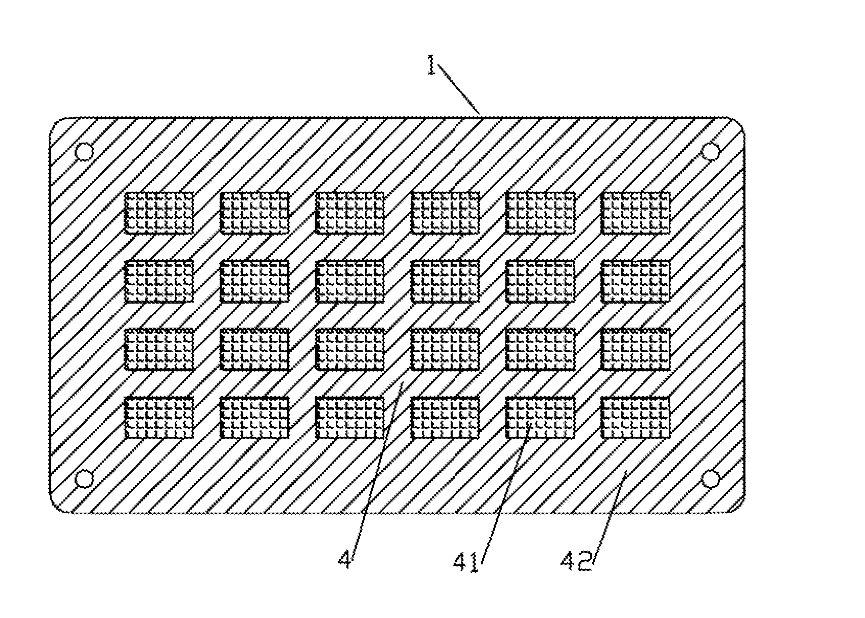
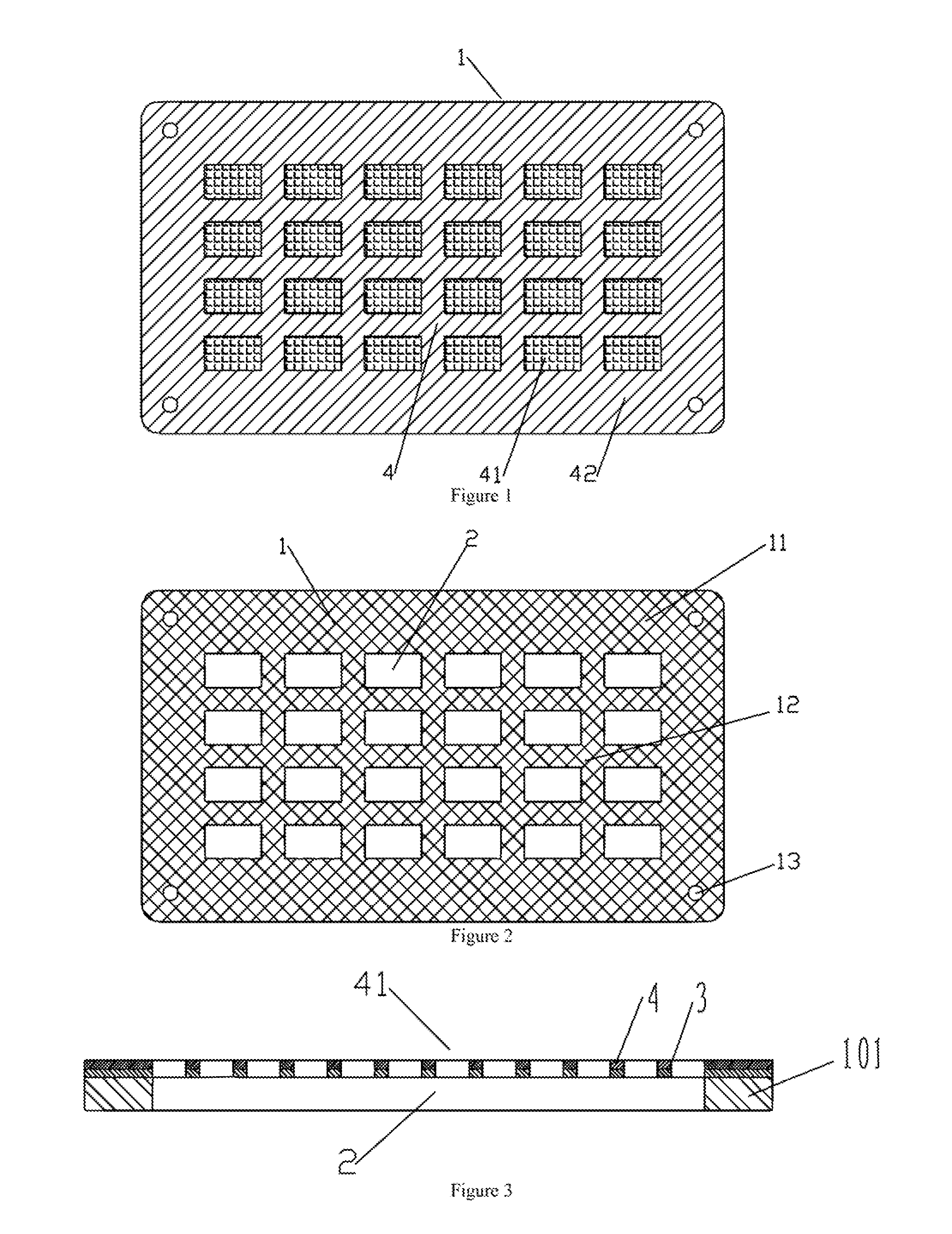
[0034]4. Develop the top photoresist layer (202) formed in the step 3, and wash away the soluble composition until the surface of invar steel substrate (101) of pattern region (41) and frame region (42) (include an outside border area and an inside separation area) are exposed to ...
second embodiment
The Second Embodiment
[0044]Second embodiment of manufacturing an fine metal mask used in OLED production includes the following steps:
[0045]1. Clean 1.2 mm±5 μm stainless steel, substrate (101) by acid, organic solvent and deionized water ultrasonic about 15 min, and then drying in clean drying box.
[0046]2. Coat the top and bottom surface of the stainless steel substrate (101) with a 45 μm photoresist layer (202), and cover the bottom photoresist layer (202) with a layer of photoresist protective film (203).
[0047]3. Attach a film (or mask) (9) to the top photoresist layer (202), then expose using the parallel light (6) from a parallel exposure machine.
[0048]4. Attach a film (or mask) (9) to the bottom photoresist layer (202), then expose using the parallel light (6) from a parallel exposure machine.
[0049]5. Develop the top photoresist layer (202) formed in step 4, and wash the soluble composition away until the pattern region (41) on the surface of the stainless steel substrate (101...
third embodiment
The Third Embodiment
[0059]Third embodiment of manufacturing a fine metal mask used in OLED production includes the following steps:
[0060]1. Clean a 1.5 mm±5 μm invar steel substrate (101) by acid, organic solvent and deionized water ultrasonic about 15 min, and then drying in clean drying box.
[0061]2. Coat the top and bottom surface of the invar steel substrate (101) with a 50 μm photoresist layer (202), and cover the bottom photoresist layer (202) with a layer of photoresist protective film (203).
[0062]3. Expose the top photoresist layer (202) by the parallel light (6) from a laser direct image exposure system (Patterns that need to be exposed through light have been imported into a computer).
[0063]4. Expose the bottom photoresist layer (202) by the parallel light (6) from a laser direct image exposure system (Patterns that need to be exposed through light have been imported into a computer).
[0064]5. Develop the top photoresist layer (202) formed in step 4, and wash the soluble com...
PUM
| Property | Measurement | Unit |
|---|---|---|
| Length | aaaaa | aaaaa |
| Length | aaaaa | aaaaa |
| Length | aaaaa | aaaaa |
Abstract
Description
Claims
Application Information


