

Glass-ceramics substrates for graphene growth
a glass-ceramic substrate and graphene technology, applied in the direction of crystal growth process, chemically reactive gas, chemical vapor deposition coating, etc., can solve the problems of large-scale synthesis route for the production of high-quality graphene at low cost, substantially hampered the proliferation of the technology
- Summary
- Abstract
- Description
- Claims
- Application Information
AI Technical Summary
Benefits of technology
Problems solved by technology
Method used
Image

Examples
example 1
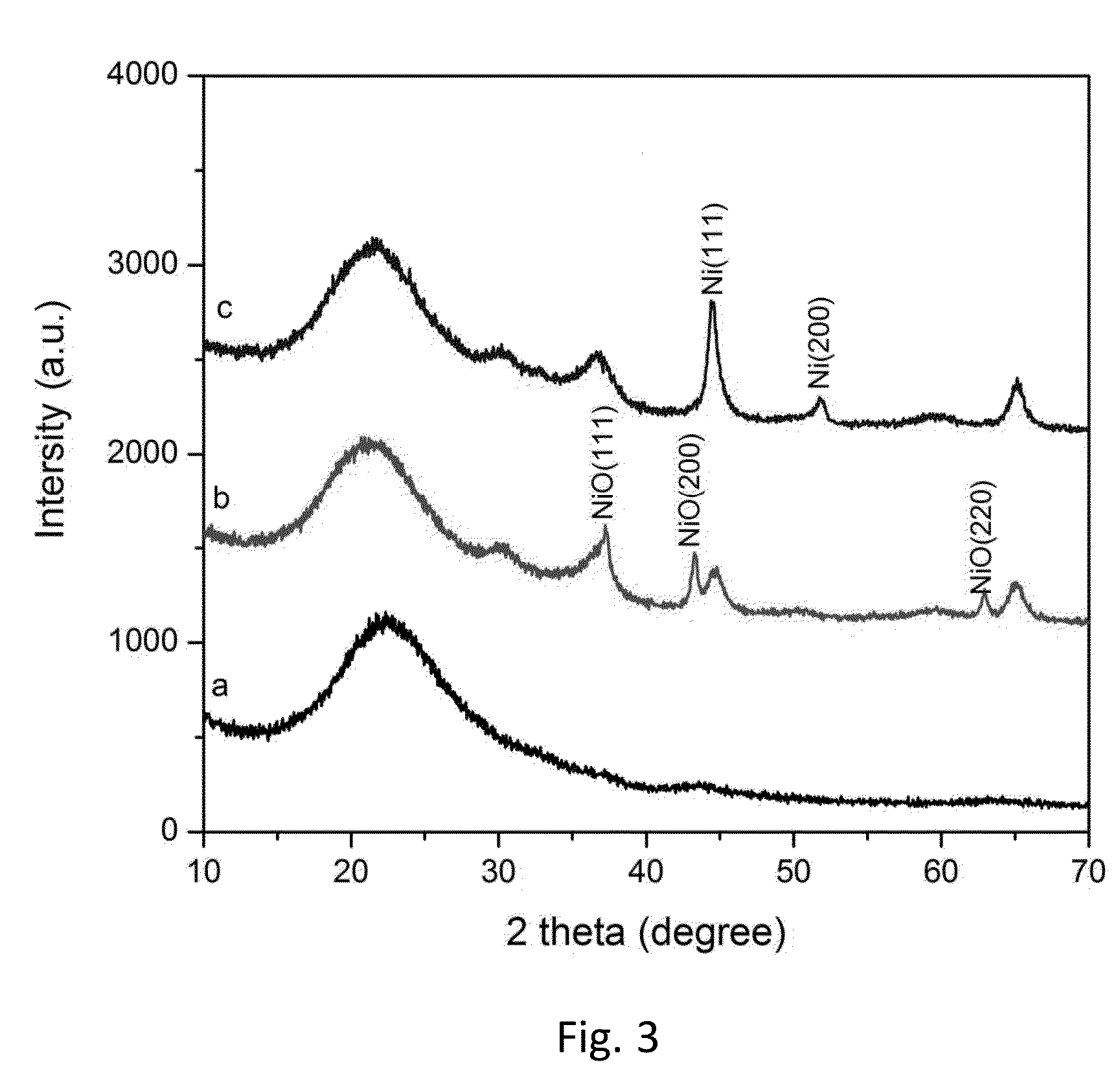
Single / Bi-Layer Graphene Growth on Ni-Containing Glass-Ceramics
[0038]A glass-ceramic substrate having the composition summarized in Table 1 (Example 1) is heat-treated in air at 750° C. for 2 hr, followed by 850° C. for 4 hr. The sample is then heated in H2 at ambient pressure at 450° C. for 5 hr.
[0039]Glancing angle x-ray diffraction (XRD) data from the surface of the glass-ceramic (a) as-prepared, (b) after heating in air, and (c) after heating in hydrogen are shown in FIG. 3.
[0040]Reflections that index to NiO appear following oxidation, and reflections that index to metallic Ni are observed after H2 reduction. In FIG. 3c, peaks located at 44.35° and 51.33° correspond to face-centered cubic Ni (111) and Ni (200), respectively.
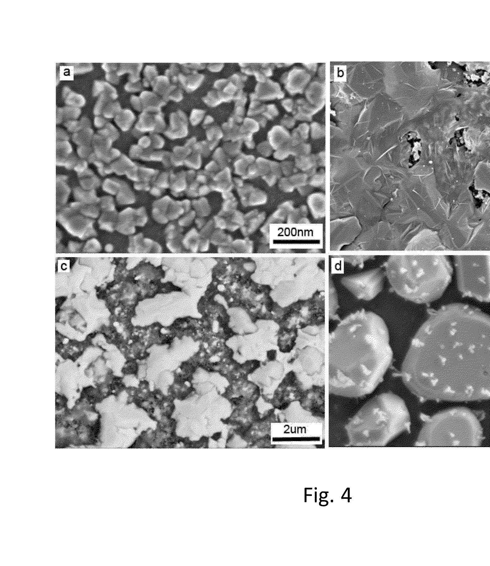
[0041]A scanning electron microscope (SEM) micrograph of the glass-ceramic surface showing 50-100 nm Ni nanoparticles on the surface is shown in FIG. 4a. The metal nanoparticles comprise a plurality of discrete islands. A surface conductivity measurement sho...
example 2
In-situ Growth of Graphene on Glass-Ceramics Without Pre-Reduction
[0056]The Example 1 glass-ceramic substrate was heated in air at 780° C. for 2 hr, and then at 1000° C. for 2 hr to form nickel oxide. No pre-reduction in hydrogen gas was performed prior to graphene growth.
[0057]Graphene was grown without pre-reduction at CVD conditions of 1000° C. and 5×10⁻⁵ Torr in C2H2 / H2. The in situ reduction of nickel oxide to nickel metal is believed to have occurred during the CVD growth as a result of the CVD growth conditions. An SEM micrograph and Raman spectra map are shown in FIG. 7a and FIG. 7b, respectively. Color drawings for the Raman maps are not provided.
example 3
Graphene Growth on Ni Glass-Ceramics Thermally-Treated in N2
[0058]FIG. 8 shows data for graphene grown on the Example 1 glass-ceramic substrate, which was heat-treated in nitrogen at 780° C. for 2 hr, followed by 1000° C. for 2 hr. The sample is then heated in H2 at ambient pressure at 450° C. for 5 hr. Graphene was formed following the pre-reduction in hydrogen at CVD conditions of 1000° C. and 5×10⁻⁵ Torr in C2H2 / H2.
[0059]As seen with reference to the SEM micrographs in FIG. 8a and FIG. 8b, graphene was formed primarily on the surface of localized Ni particles. The Ni particles were formed in situ during the graphene growth. Raman spectra (FIG. 8c) show G and 2D peaks for graphene formed on the Ni particles (top two curves). The lower curve shows only weak Raman reflections for areas of the surface between the Ni particles. In FIG. 8d, most G / 2D ratio (>0.5) mapping indicates that the graphene growth (and graphene thickness) is not uniform across the surface. Monolayer and primar...
PUM
| Property | Measurement | Unit |
|---|---|---|
| Nanoscale particle size | aaaaa | aaaaa |
| Electrical conductor | aaaaa | aaaaa |
| Metallic bond | aaaaa | aaaaa |
Abstract
Description
Claims
Application Information