Optical device

a technology of optical devices and optical components, applied in the direction of solid-state devices, semiconductor devices, radio-controlled devices, etc., can solve the problems of high absorption, and not eliminating the long path lengths of led chips, so as to achieve high optical efficiency, high electrical wall plug efficiency, and high efficiency

Active Publication Date: 2015-08-20
META PLATFORMS TECH LLC
View PDF3 Cites 43 Cited by
  • Summary
  • Abstract
  • Description
  • Claims
  • Application Information

AI Technical Summary

Benefits of technology

[0071]Where the structure of the semiconductor material is free-standing and does not include any of these hard materials it is possible to structure both sides of the semiconductor material. The sub-mesa is defined at a precise position relative to the mesa, i.e. the central axis of the mesa and sub-mesa are ideally common. In very general terms, this can be considered a dual lens system. This design allows the light advantageously directed by the first structure toward the second surface to exit as previously described on a planar surface, whilst also allowing light at greater angles than the perpendicular to be also extracted through the exit surface shaped as the sub-mesa.
[0072]The combination of the micro-LED structure and the exit surface sub-mesa structure create a highly efficient design that can be realised even if the aspect ratio of the micro-LED mesa is reduced. This is advantageous to achieve high electrical wall plug efficiency (WPE) as well as high optical efficiency because the area of the semiconductor generating light remains relatively high. In this case, the current densities used to drive the light generating regions can be similar to conventional LED devices. Overall, a high total optical flux, high extraction efficiency and relatively narrow beam profile can be achieved that are improvements in existing device designs where at least one surface is still essentially planar.

Problems solved by technology

A major challenge in the field of LEDs is to extract as much of the emitted light as possible from the semiconductor material into the surrounding medium, which may be air.
There are a number of problems with traditional cuboid-shaped LEDs including: 1) most light emitted from the active layer is outside the angle of total internal reflection, which leads to long path lengths for rays; and 2) they suffer from high absorption due to increased path lengths
However, it does not eliminate the long path lengths within the LED chip, nor the requirement for an external mirror.
Also, the technique is less suitable to the widely used gallium nitride (GaN) based LEDs.
The reason for this is that the sapphire and silicon carbide (SiC) substrates commonly used in GaN-based LED chips are very hard materials and are very difficult to shape mechanically, for example, with a dicing saw.
In LEDs comprising these materials, it seems not to be a practical solution to shape the whole chip.
Total internal reflection is a common problem for LED devices, as the refractive index of the substrate materials used is typically much greater than air, which typically surrounds the LED.
The design challenge is to create a structure which allows more light to be extracted into the air.
However, there are limitations to this planar surface roughening approach.
Firstly, the design still results in multiple internal reflections before the light escapes.
This results in losses, especially reflections on the contact electrodes, even if the reflections are relatively efficient.
Secondly, the design typically includes mirrors as part of the electrical contact on the planar surface to enhance the light extraction.
For the larger and higher power devices, the design requirements mean the material properties of the sapphire substrate become more limiting.
Sapphire has a poor thermal conductivity, so the device becomes hotter as the substrate becomes thicker.

Method used


Image

  • Optical device
  • Optical device
  • Optical device

Examples


Embodiment Construction

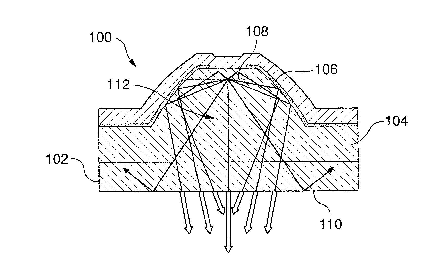
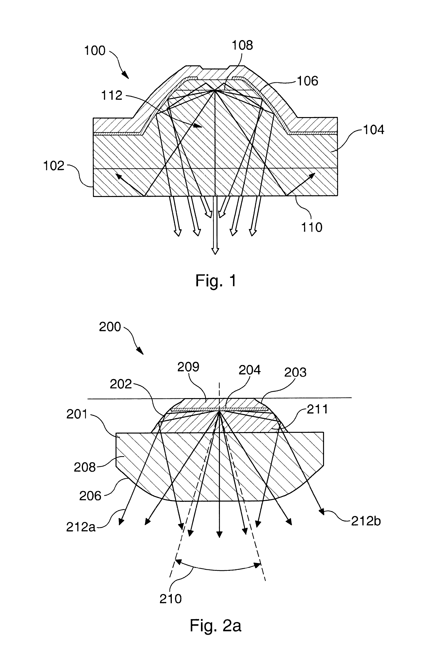
[0081]It is noted that the following description refers predominantly to LED devices but the invention should not be limited to such. The invention applies equally to light receiving devices, such as photodiodes. Further, in this specification the term “light” will be used in the sense that it is used in optical systems to mean not just visible light, but also electromagnetic radiation having a wavelength outside that of the visible range.

[0082]For micro-LED structures having an active layer enclosed in a mesa structure, the applicant has identified a relationship between the geometrical dimensions of the mesa, the total amount of light generated and the amount of light extracted. In the case of a micro-LED, the directionality (beam profile), is directly linked to the material properties and the difference in refractive indices between the material of the LED and the surrounding medium. The applicant has therefore established that the main areas to improve in a micro-LED design are ...


PUM


Abstract

An optical device and method for fabricating an optical device. The optical device comprising: a semiconductor material comprising an active layer configured to emit light when an electrical current is applied to the device and/or to generate an electrical current when light is incident on the active layer, wherein the semiconductor material comprises a first surface and an opposed second surface, from which light is emitted from and/or received by the device, and wherein the first surface defines a first structure comprising the active layer and configured to reflect light emitted from the active layer toward the second surface and/or to reflect light received by the device toward the active layer, and the second surface defines a second structure configured to permit light incident on the second surface at an angle outside a critical angle range to the planar normal to pass therethrough.

Description

TECHNICAL FIELD[0001]The invention relates to an optical device. Specifically, the invention relates to, but is not limited to, an optical device with efficient coupling of light between the device and the environment. In specific exemplary devices, the invention relates to, but is not limited to, a light emitting diode (LED) having an improved extraction efficiency (EE).BACKGROUND OF THE INVENTION[0002]LEDs convert electrical energy into optical energy. In semiconductor LEDs, light is usually generated through recombination of electrons, originating from a first doped semiconductor layer, and holes, originating from a second doped semiconductor layer. In some infra-red emitting semiconductor materials light can be generated by electron intersub-band transitions rather than electron-hole transitions. The area where the main light generation takes place is referred to herein as the active layer, or more generally as the active region.[0003]A major challenge in the field of LEDs is to...

Claims


Application Information

Patent Timeline
Patent Type & Authority Applications(United States)
IPC IPC(8): H01L33/24H01L31/0232H01L33/60H01L27/144H01L33/00H01L31/0352H01L33/58H01L33/32H01L31/18H01L27/15
CPCH01L33/24H01L31/1856H01L31/02327H01L33/60H01L27/1446H01L33/0075H01L31/0352H01L33/58H01L33/32H01L27/153H01L31/02325H01L33/20H01L33/46H01L31/0547Y02E10/52H01L27/156H01L31/0232H01L2933/0025
Inventor SHEPHERD, NICK
Owner META PLATFORMS TECH LLC
Why Eureka
Try Eureka