
Semiconductor device

a semiconductor and device technology, applied in semiconductor lasers, instruments, optical elements, etc., can solve the problems of non-trivial monolithic integration of iii-v based light sources on silicon platforms, time-consuming and difficult to achieve relatively high-precision alignment, and achieve easy integration/implementation, widening a range of applications/optical systems, and easy fabrication and/or integration.

Active Publication Date: 2015-10-15
IBM CORP
View PDF1 Cites 17 Cited by
  • Summary
  • Abstract
  • Description
  • Claims
  • Application Information

AI Technical Summary

Benefits of technology

The present invention provides an optical device with improved efficiency and optical performance. The optically active material is grown in a predefined structure within the optically passive aspect, which increases the overlap of the generated light and the light transmission / guiding material. This results in higher material gain, improved modal gain, and lower threshold currents, leading to better optical performance. The predefined structure can be easily implemented without additional bonding and alignment processes. A desirable feature is the use of a lateral cavity design with azimuthal symmetry and high quality factor values. The photonic structure comprises a wire waveguide and at least a tapered region to further improve the modal gain. Overall, the present invention offers greater efficiency and improved optical performance compared to previously-proposed devices.

Problems solved by technology

A problem in this regard is that, due to the indirect band-gap of silicon, no silicon-based light sources are available and / or may be used.
However, an associated problem in this regard is posed by the lattice mismatch between III-V compound semiconductors and silicon, making the direct, monolithic integration of III-V based light sources on a silicon platform non-trivial.
In this regard, it may be time-consuming and challenging to achieve relatively high-precision alignment when bonding a pre-processed III-V based light source to a given waveguide structure, particularly since the alignment precision may be further limited by the bonding process.
Because the alignment accuracy of light sources based on compound semiconductor systems, such as, for example, III-V materials, with respect to optical structures, such as, for example, silicon waveguides and / or resonators, may be rather dependent on lithography accuracy, it may be insufficient for certain applications.
Generally, the positioning accuracy of such heterogeneously / hybrid integrated optical systems is inherently lower compared to monolithic integration.
Furthermore, concerning yield, heterogeneous / hybrid integration may not match the standards provided by integrated electronics.
A further problem to be considered for heterogeneous / hybrid optical systems, particularly for III-V based light sources used with silicon photonics, is concerned with how the generated light is located in such systems.
In this regard, it may be that the light is located mainly in the silicon with a relatively smaller overlap with the III-V material system, which may result in a relatively low material gain and high threshold currents.
Or, it could be that the light is located mainly in the III-V material system in which case there is a relatively good overlap with the gain sections but also the possibility of lossy resonators that may contribute to relatively lower optical output power.
Such problems are related to the lattice mismatch and difference in thermal coefficients between III / V material systems and silicon.
However, neither of these documents address the problems, as discussed hereinabove, with respect to hybrid / heterogeneous integrated optical systems and / or the monolithic integration and optical coupling of light sources with optical structures such as waveguides and, more generally, photonic structures.
These documents do not seem to address the monolithic integration of III-V based light sources on a silicon platform.
Furthermore, they do not address / propose any solution / alternative to the problems and / or issues associated with hybrid / heterogeneous integrated optical systems.
Furthermore, this document does not seem to provide instruction on how to address the problems / issues associated with hybrid / heterogeneous integrated optical systems as hereinbefore described.
Whilst suitable for organic gain material, spin-coating is not compatible with respect to solid state gain materials, such as, for example, III-V material systems.
Furthermore, this document does not disclose any electrical pumping.
Operation at <1200 nm seems to be described which may make the disclosed device unattractive for light propagation using silicon waveguides, for example.
Also, this document does not seem to provide instruction on how to address the problems / issues associated with hybrid / heterogeneous integrated optical systems as hereinbefore described.
Such a hybrid mode of operation may cause relatively higher threshold currents and lower optical output levels.
Based on the index contrasts of the fabricated structures, it may be that the light generated by the laser source / compound semiconductor aspect is mainly confined in the silicon with a relatively small proportion being confined within the compound semiconductor, which may serve to limit the efficiency of the laser and result in relatively increased power consumption.
It does not address the monolithic integration of a light / laser source based on a compound semiconductor such as, a III-V material system, with respect to an optical structure such as, a photonic structure and / or optical waveguide based on a silicon platform.
This document does not address how a compound semiconductor based light source may be monolithically integrated with respect to integrated optics based on a silicon platform.
Furthermore, the lattice compatible layer has to be bonded to the upper silicon dioxide layer, which may increase the number of processing steps and / or complexity in the fabrication of the device disclosed in this document.
Accordingly, it is a challenge to provide a semiconductor device for use in any given optical application that provides an improved performance, particularly in respect of lower threshold currents and / or higher optical output power, over previously-proposed optical systems, for example, those based on heterogeneous / hybrid integrated optical systems as above-discussed.
It is also a challenge that, in respect of such a semiconductor device, an optically active aspect based on a compound material system, such as, for example, a III-V material system, is directly and monolithically integrated on an integrated optical platform based on silicon, for example.

Method used


Image

  • Semiconductor device
  • Semiconductor device
  • Semiconductor device

Examples


Embodiment Construction

[0059]Within the description, the same reference numerals or signs have been used to denote the same parts or the like.

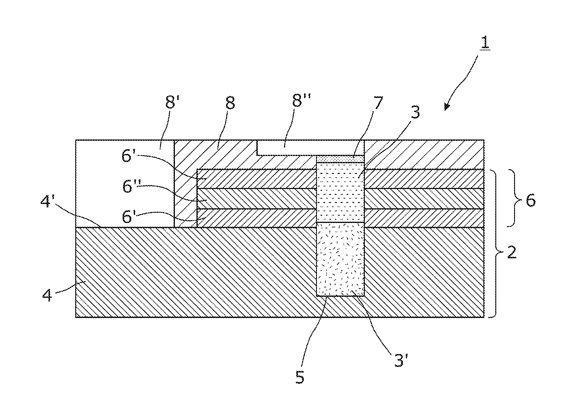
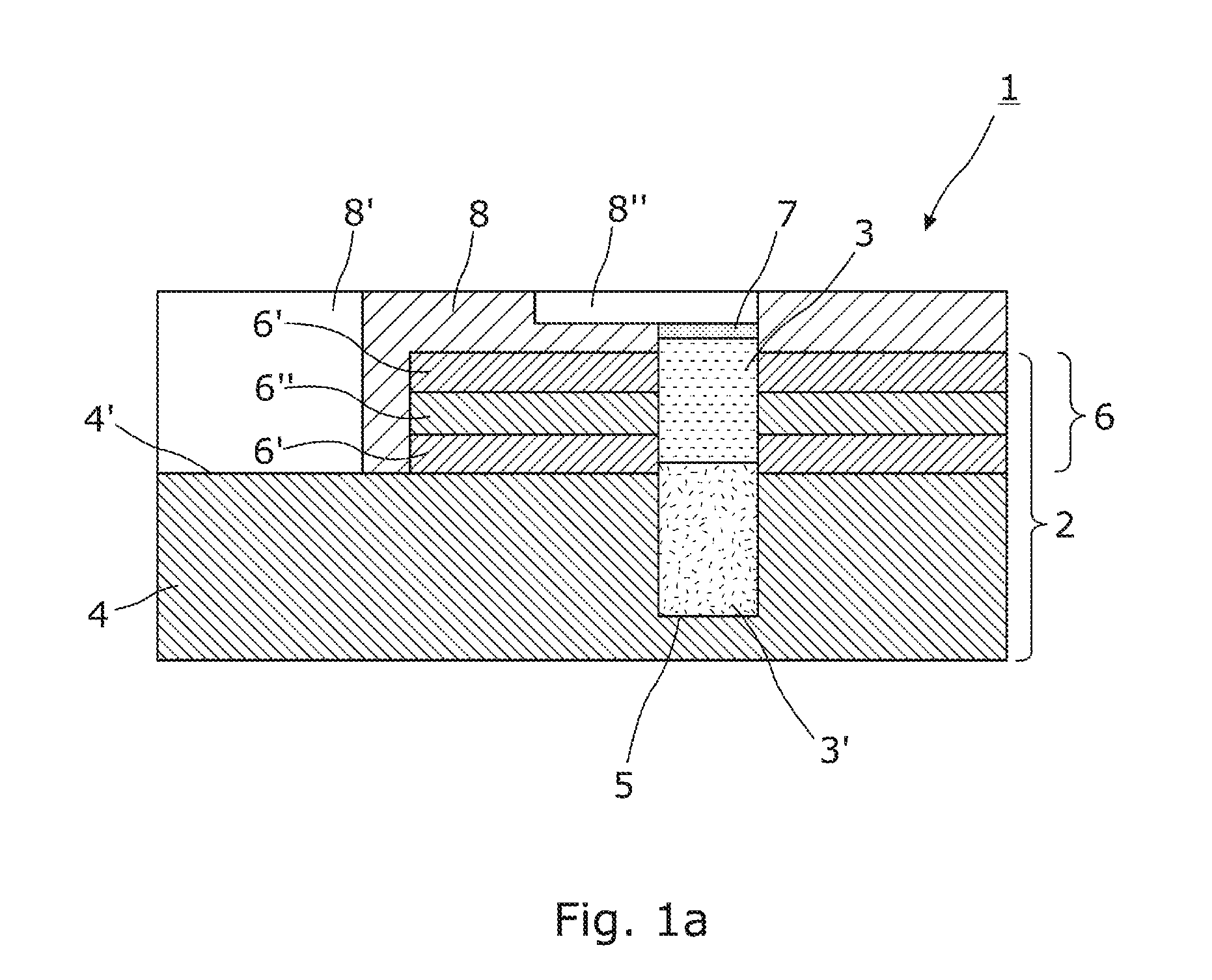
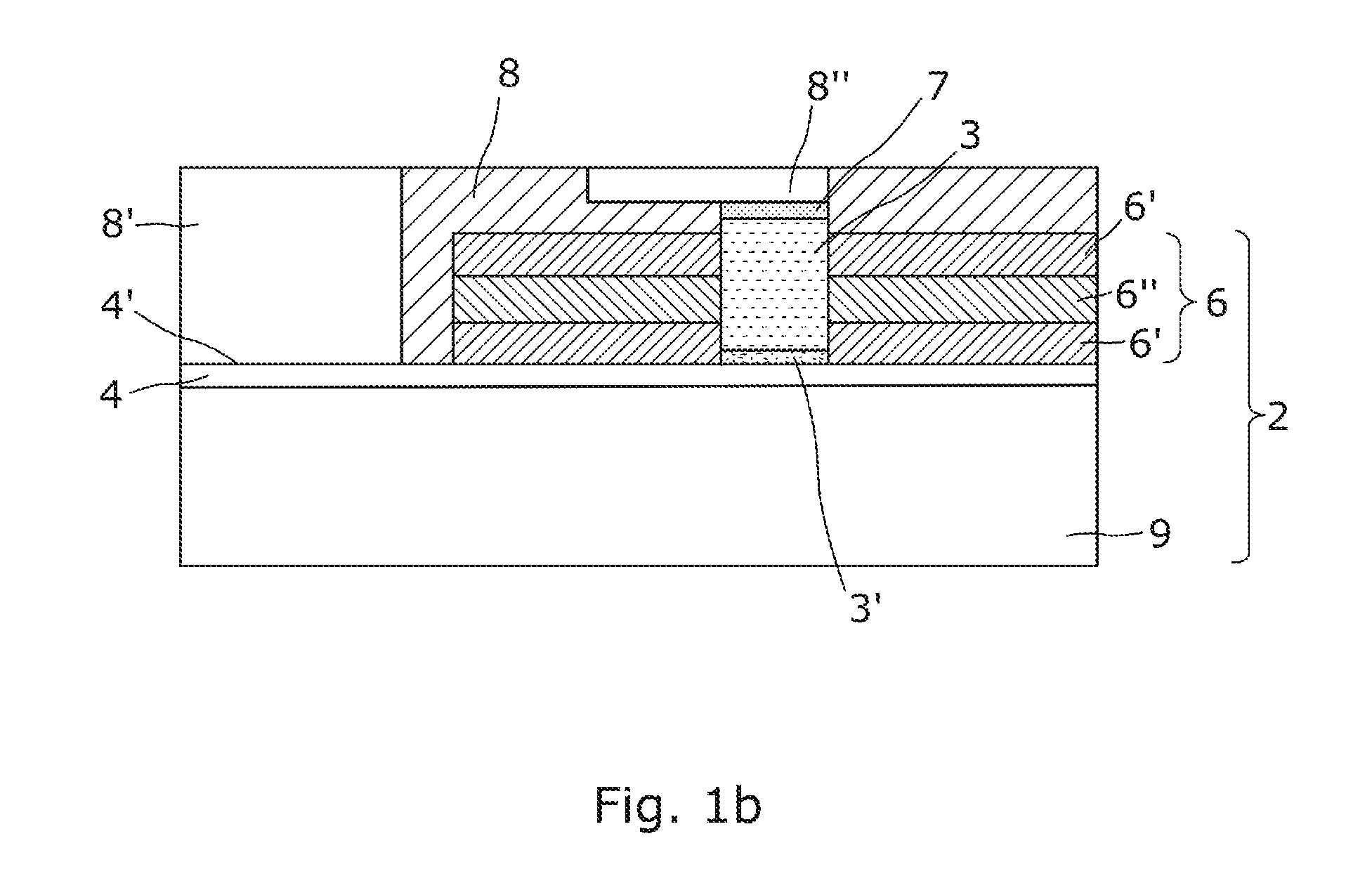
[0060]Reference is now made to FIG. 1a showing a semiconductor device 1 according to an embodiment of a first aspect of the present invention comprising at least an optically passive aspect or region 2 that, when the semiconductor device 1 is in use, is operable in substantially an optically passive mode for the transmission and / or coupling of light from a given location to a desired location, rather than for the generation, amplification, detection and / or modulation of light. The optically passive aspect 2 is structured thereby to comprise at least a predefined structure 5, which extends to at least an upper surface 4′ of a crystalline seed layer 4 provided in respect of the optically passive aspect 2 or even into the crystalline seed layer 4 as for a given embodiment of the present invention as shown in FIG. 1a. There is also provided at least an optically active ...


PUM


Abstract

The present invention relates to a semiconductor device (1) for use in at least an optical application comprising: at least an optically passive aspect (2) that is operable in substantially an optically passive mode, and at least an optically active material (3) comprising at least a material that is operable in substantially an optically active mode, wherein: the optically passive aspect (2) further comprises at least a crystalline seed layer (4), the optically active material (3) being epitaxially grown in at least a predefined structure (5) provided in the optically passive aspect (2) that extends to at least an upper surface (4′) of the crystalline seed layer (4), and the optically passive aspect (2) is structured to comprise at least a passive photonic structure (6), wherein the crystalline seed layer (4) comprises a crystalline wafer and wherein the optically active material (3) comprises at least one of: a III-V material and a II-VI material.

Description

FIELD OF THE INVENTION[0001]The present invention relates to a semiconductor device for use in an optical application and a method of fabrication therefor.BACKGROUND OF THE INVENTION[0002]In order to meet the requirements of future computing systems, higher speed and more energy efficient alternatives to electrical interconnects such as, for example, on-chip optical interconnects and chip-to-chip optical interconnects, may be needed. Integrated optics, particularly silicon photonics, may suitably meet such needs. For the cost-effective, mass-fabrication of complementary metal-oxide semiconductor (CMOS)-based chips having a performance capability suitable for use in high-speed devices and / or applications, integrated optical interconnects with compatible light sources are to be provided. A problem in this regard is that, due to the indirect band-gap of silicon, no silicon-based light sources are available and / or may be used. This problem has been addressed by the use of III-V based se...

Claims


Application Information

Patent Timeline
IPC IPC(8): G02B6/12G02B6/13G02B6/122
CPCG02B6/12004G02B6/131G02B6/122G02B6/1225G02B6/42G02B6/43H01L31/02327H01S5/005H01S5/026H01S5/183H01S5/11H01L33/10
Inventor CZORNOMAZ, LUKASHOFRICHTER, JENSRICHTER, MIRJARIEL, HEIKE
Owner IBM CORP
Learn More