Method for Improving E-Beam Lithography Gate Metal Profile for Enhanced Field Control

Active Publication Date: 2015-10-29
NXP USA INC
View PDF0 Cites 43 Cited by
  • Summary
  • Abstract
  • Description
  • Claims
  • Application Information

AI Technical Summary

Problems solved by technology

Attempts to reduce gate leakage current in such devices may adversely affect other device properties.
In addition, the gate electrode device features at the edges of deep submicron gates

Method used


Image

  • Method for Improving E-Beam Lithography Gate Metal Profile for Enhanced Field Control
  • Method for Improving E-Beam Lithography Gate Metal Profile for Enhanced Field Control
  • Method for Improving E-Beam Lithography Gate Metal Profile for Enhanced Field Control

Examples


Embodiment Construction

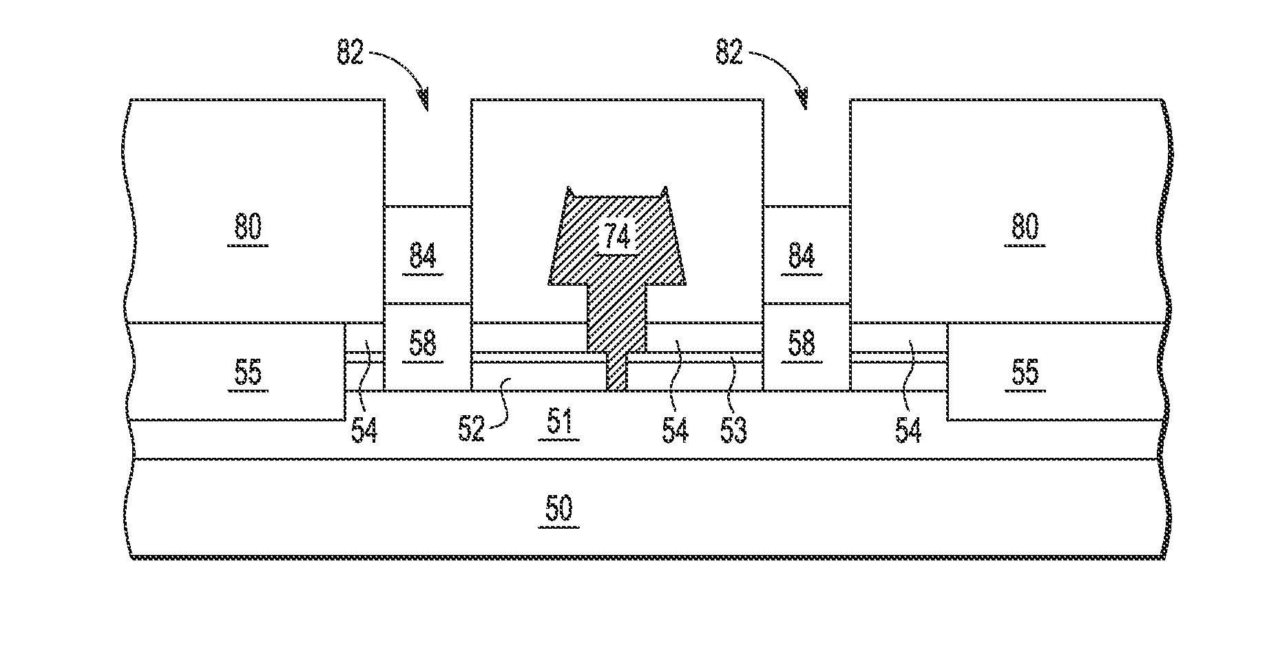
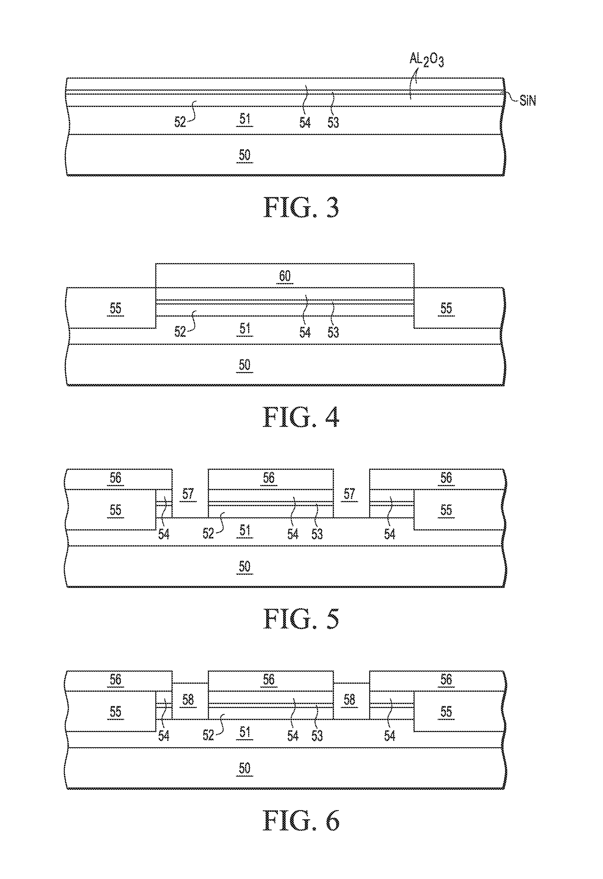
[0011]A high frequency, high voltage semiconductor device, such as a gallium nitride field effect transistor device or diode, and associated fabrication process are described for providing enhanced field control at the edges of deep submicron gates by fabricating the gate metal profile to include a stepped field plate gate structure with a process that is integrated into an existing e-beam lithography flow. In selected embodiments, a Schottky gate electrode structure is formed with lower gate ledges and upper extensions by using a patterned multi-layer resist stack to define stepped openings in a multi-layer passivation surface stack in the course of etching a gate contact opening to expose the underlying gallium nitride substrate surface. During formation of the stepped field plate gate electrode structure, a multilayer dielectric stack (Al2O3 / SiN / Al2O3) is sequentially deposited on a gallium nitride substrate wafer to form a dielectric passivation stack in which openings are etche...


PUM


Abstract

A semiconductor device is provided which includes a GaN-on-SiC substrate (50-51) and a multi-layer passivation stack (52-54) in which patterned step openings (76) are defined and filled with gate metal layers using a lift-off gate metal process to form a T-gate electrode (74) as a stepped gate electrode having sidewall extensions and a contact base portion with one or more gate ledges.

Description

BACKGROUND OF THE INVENTION[0001]1. Field of the Invention[0002]The present invention is directed in general to integrated circuit devices and methods for manufacturing same. In one aspect, the present invention relates to the manufacture and use of field effect transistor devices.[0003]2. Description of the Related Art[0004]Semiconductor devices used in high-efficiency power amplifier (HEA) applications require higher speed and power handling capability. To meet these operating requirements, high power semiconductor devices may be formed with semiconductor materials, such as gallium nitride (GaN), having material properties that are suitable for use in such applications. For example, high speed transistor switch devices, such as high electron mobility transistor (HEMT) devices, formed with GaN-based materials offer many advantages in RF applications, especially in HEA applications, by delivering high current, high breakdown voltage, and high unity gate current cutoff frequency (fT)...

Claims


Application Information

Patent Timeline
IPC IPC(8): H01L21/285H01L29/20H01L29/778H01L29/423
CPCH01L21/28587H01L21/28581H01L29/778H01L29/2003H01L29/42312H01L29/42316H01L29/66462H01L29/7786H01L29/40114
Inventor MOORE, KAREN E.GREEN, BRUCE M.
Owner NXP USA INC
Why Eureka
Try Eureka