Three-Dimensional Crystalline, Homogenous, and Hybrid Nanostructures Fabricated by Electric Field Directed Assembly of Nanoelements

Inactive Publication Date: 2015-11-12
NORTHEASTERN UNIV
View PDF10 Cites 14 Cited by
  • Summary
  • Abstract
  • Description
  • Claims
  • Application Information

AI Technical Summary

Benefits of technology

This patent text discusses a method for increasing the speed, amount, or degree of formation of nanostructures by using an electric field to assemble nanoelements. The method involves increasing the electric field used for assembly, decreasing the frequency of the AC component of the field, increasing the force acting on the nanoelements, increasing the concentration of nanoelements, decreasing the size or density of the via in which the nanoelements are assembled, and increasing the size of the nanoelements. These techniques can help to improve the speed and accuracy of nanostructure formation.

Problems solved by technology

In these assembly processes, the two electrodes required for applying an electric field are usually on the same substrate or very close to each other (order of microns), making the fabrication techniques unsuitable for specific applications such as interconnects in complementary metal-oxide-semiconductor (CMOS) based devices (International Technology Roadmap For Semiconductors 2007 Edition Interconnecf.
However, the process provided no control over the length of the nanorods, impeding the potential use of the rods in sensors and CMOS interconnect applications.
However, these high temperature processes are not compatible with CMOS technology (Maury et al., Adv.
For local vertical interconnects, the methods that have been carried out are not highly scalable.
Previously available directed assembly techniques have not demonstrated the ability to make solid homogeneous or hybrid crystalline nanostructures with nanoscale precision, and also do not enable assembly of larger diameter (e.g., 200 nm or above) nanostructures with nanoscale precision, or the assembly of nonconducting nanoparticles.

Method used


Image

  • Three-Dimensional Crystalline, Homogenous, and Hybrid Nanostructures Fabricated by Electric Field Directed Assembly of Nanoelements
  • Three-Dimensional Crystalline, Homogenous, and Hybrid Nanostructures Fabricated by Electric Field Directed Assembly of Nanoelements
  • Three-Dimensional Crystalline, Homogenous, and Hybrid Nanostructures Fabricated by Electric Field Directed Assembly of Nanoelements

Examples


example 1

Particle and Template Preparation

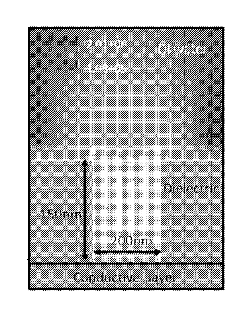
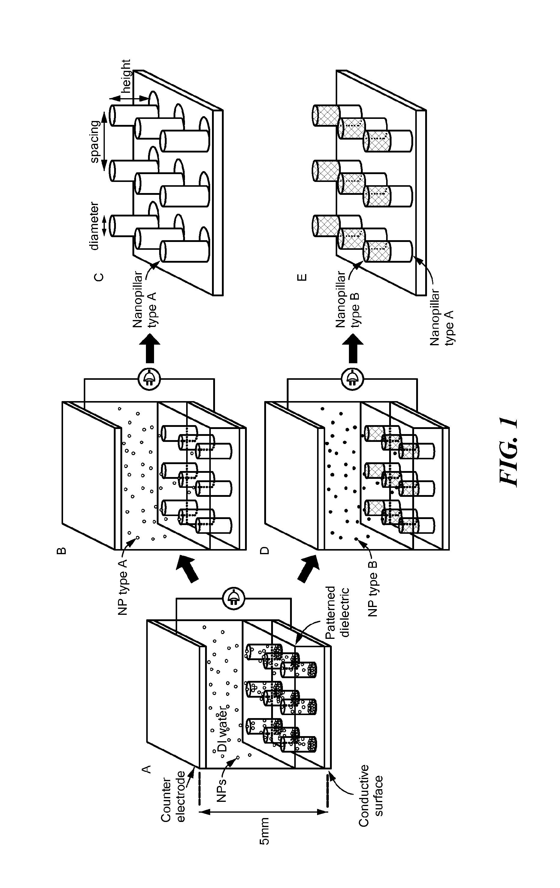
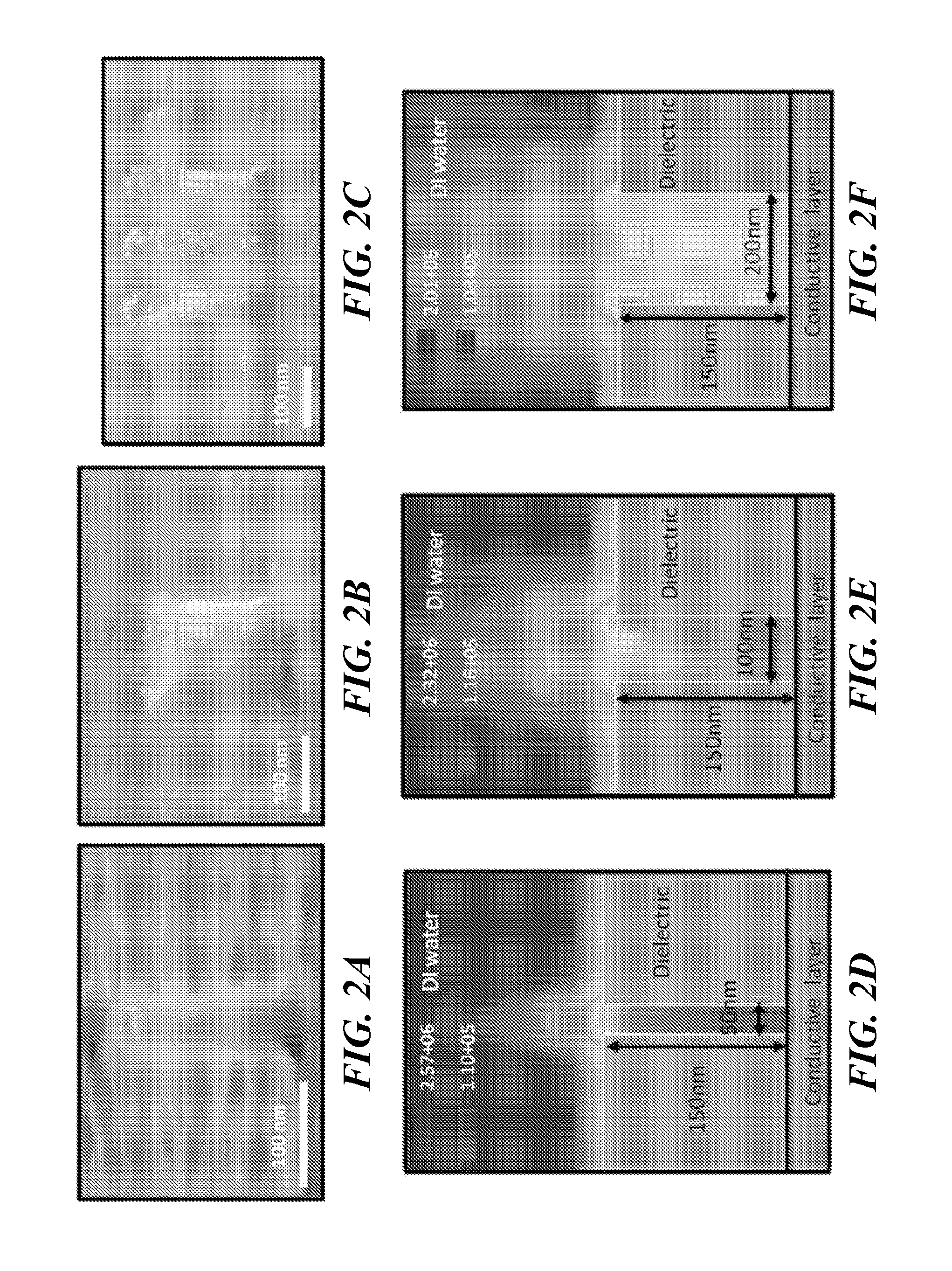
[0114]Aqueous gold NPs (nominal diameter: 5 nm) were purchased from British Biocell International. Aqueous copper NP suspension (nominal diameter: 10 nm) was purchased from Meliorium Technologies (Rochester, N.Y.). Aqueous fluorescent polystyrene-latex (PSL) NP suspension (Fluoro-Max Red, nominal diameter: 22 nm) was purchased from Thermo Scientific (Waltham, Mass.). Aqueous polystyrene fluorescent silica NP suspension (fluorescent-green, nominal diameter: 30 nm) was purchased from Kisker-biotech (Steinfurt, Germany). The template depicted in FIG. 1 was prepared by sputtering Cr / Au (2 nm / 120 nm) onto a SiO2 / Si (470 nm / 380 μm) wafer followed by dicing the wafer into 12 mm×12 mm chips. The Cr / Au chips were cleaned with piranha solution (H2SO4 / H2O2, 2:1) and spin-coated with PMMA. Nanoscale patterns were fabricated using conventional electron beam lithography and developed subsequently with methyl isobutyl ketone and isopropyl alcohol (MIBK / IPA, 1:3).

example 2

Nanoparticle-Based Nanopillar Manufacturing

[0115]The template prepared as described in Example 1 and a counter electrode (Cr / Au sputtered gold) were connected to a function / arbitrary waveform generator (Agilent 33220A) and submerged into a NP suspension. Following the application of a sinusoidal AC electric field with or without a DC offset, the template and the planar counter electrode were removed from the suspension using a dip coater (KSV NIMA) at a controlled speed (85 mm / min) Finally, the PMMA layer on the template was removed using acetone for metallic and silica nanopillars, or ethanol for PSL nanopillars.

example 3

Nanopillar Electroplating Process

[0116]Techni-Gold 25 ES RTU (ready-to-use) solution was purchased from Technic, Inc. (Pawtucket, R.I.). The solution included sulfuric acid, ethylenediamine, sodium gold sulfite and sodium sulfite. The temperature of the solution was held at 60° C. The patterned template and a counter electrode were submerged into the electroplating solution. In contrast to the directed assembly, a platinized titanium mesh was used as the counter electrode. The solution was heated at a set temperature of 60° C., while stirring with a magnetic stirrer at a set rate of 75 rpm. A DC voltage was applied between the template and the counter electrode using a Keithley 2400 source meter. The magnitude of the applied voltage and duration of deposition were altered to control the electroplating rate.


PUM

PropertyMeasurementUnit
Temperatureaaaaaaaaaa

Abstract

A variety of homogeneous or layered hybrid nanostructures are fabricated by electric field-directed assembly of nanoelements. The nanoelements and the fabricated nanostructures can be conducting, semi-conducting, or insulating, or any combination thereof. Factors for enhancing the assembly process are identified, including optimization of the electric field and combined dielectrophoretic and electrophoretic forces to drive assembly. The fabrication methods are rapid and scalable. The resulting nano structures have electrical and optical properties that render them highly useful in nanoscale electronics, optics, and biosensors.

Description

CROSS REFERENCE TO RELATED APPLICATIONS[0001]This application claims the benefit of provisional application Ser. No. 61 / 666,181 filed Jun. 29, 2012 and entitled “NANOSCALE INTERCONNECTS AND COMPOSITE THREE-DIMENSIONAL NANOSTRUCTURES FABRICATED BY ELECTRICAL FIELD DIRECTED ASSEMBLY OF NANOELEMENTS”, which is hereby incorporated herein by reference in its entirety.STATEMENT REGARDING FEDERALLY SPONSORED RESEARCH OR DEVELOPMENT[0002]The invention was developed with financial support from Grant No. 0832785 from the National Science Foundation. The U.S. Government has certain rights in the invention.BACKGROUND[0003]The precise assembly of nanoscale materials in a desired location and orientation on surfaces makes it possible to fabricate various types of novel structures and devices (Baughman et al., Science, vol. 297, pp. 787-792, 2002; Daniel and Astruc Chem. Rev., vol. 104, pp. 293-346, 2004; Huang et al., Adv. Mater., vol. 21, pp. 4880-4910, 2009). Nanoparticles are model nanoscale b...

Claims


Application Information

Patent Timeline
IPC IPC(8): C25D13/18B23K31/00C25D13/22C25D13/02C25D13/12
CPCC25D13/18C25D13/02C25D13/12C25D13/22B23K31/00B81C1/00111B81B2207/056H01L21/76885H01L21/2885H01L21/76879H01L2221/1094C25D3/48C25D5/02B81B2203/0361B81C2201/0187
Inventor BUSNAINA, AHMEDYILMAZ, CIHANKIM, TAEHOONSOMU, SIVASUBRAMANIAN
Owner NORTHEASTERN UNIV
Why Eureka
Try Eureka