
Planar Structure Solar Cell with Inorganic Hole Transporting Material

Inactive Publication Date: 2016-01-07
SHARP LAB OF AMERICA
View PDF4 Cites 20 Cited by
  • Summary
  • Abstract
  • Description
  • Claims
  • Application Information

AI Technical Summary

Benefits of technology

The patent text describes a new method for making a planar structure solar cell. The method includes using an inorganic layer as an electron blocking layer between the solar cell's perovskite layer and counter electrode. This layer prevents the recombination of charges at the interface between the absorber layer and counter electrode, which can cause non-performing cells. The inorganic layer acts as a p-type wide bandgap semiconductor that can transport holes from the perovskite layer to the counter electrode. The method also includes depositing layers of metal oxide and a semiconductor absorber layer onto a transparent conductive electrode, followed by the deposition of an HTM layer and a metal electrode. The use of this inorganic layer as an electron blocking layer is important for a planar perovskite architecture. The patent also provides information on the materials used for the different layers in the solar cell. The technical effect of this method is to improve the performance and efficiency of planar structure solar cells.

Problems solved by technology

In the case of perovskite based solar cells, the recombination of charges at the interface between the absorber and counter electrode results in a non-performing cell.

Method used


Image

  • Planar Structure Solar Cell with Inorganic Hole Transporting Material
  • Planar Structure Solar Cell with Inorganic Hole Transporting Material
  • Planar Structure Solar Cell with Inorganic Hole Transporting Material

Examples


Embodiment Construction

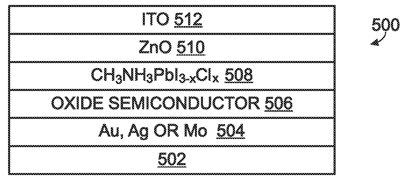
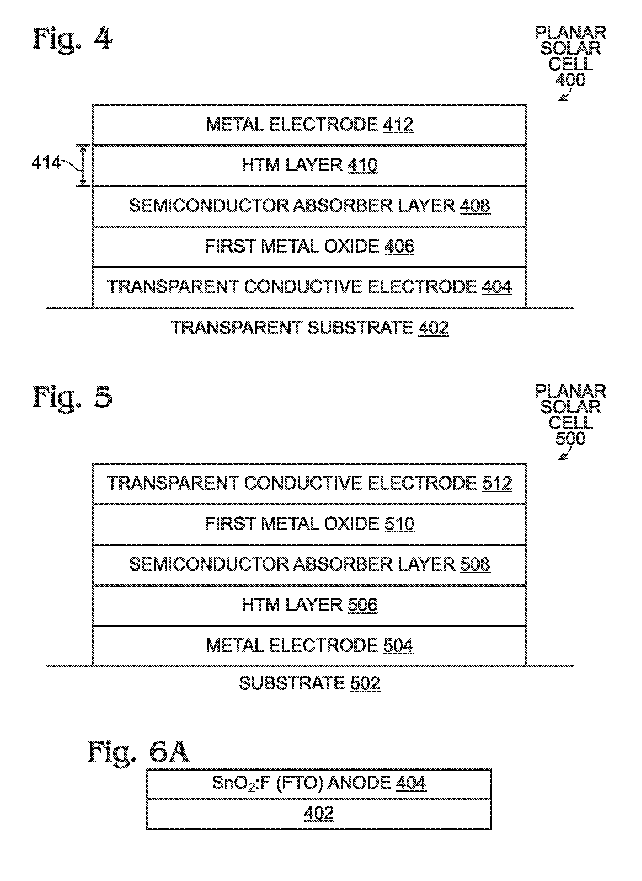
[0026]FIG. 4 is a partial cross-sectional view of a planar structure solar cell. The solar cell 400 comprises a transparent substrate 402. Silica (glass), quartz, or a plastic may be used as the transparent substrate 402. A transparent conductive electrode 404 overlies the transparent substrate 402. Fluorine-doped tin oxide (SnO2:F) can be used as the transparent conductive electrode 404. Forms of graphene, indium. tin oxide (ITO), other conductive metal oxides, and single-walled carbon. nanotubes may also possibly be used as a transparent conductive electrode material. A planar layer of a first metal oxide 406 overlies the transparent conductive electrode 404. In one aspect, the first metal oxide 406 is an n-type metal oxide. Some examples of the first metal oxide 406 include titanium oxide MOO, tin oxide (SnO2), zinc oxide (ZnO), niobium oxide (Nb2O5), tantalum oxide (Ta2O5), barium titanate (BaTiO3), strontium titanate (SrTiO3), zinc titanate (ZnTiO3), and copper titanate (CuTiO3...


PUM


Abstract

A method is provided for forming a planar structure solar cell. Generally, the method forms a transparent conductive electrode, with a planar layer of a first metal oxide adjacent to the transparent conductive electrode. For example, the first metal oxide may be an n-type metal oxide. A semiconductor absorber layer is formed adjacent to the first metal oxide, comprising organic and inorganic materials. A p-type semiconductor hole-transport material (HTM) layer is formed adjacent to the semiconductor absorber layer, and a metal electrode is formed. adjacent to the HTM layer. In one aspect, the HTM layer is an inorganic material such as a p-type metal oxide. Some explicit examples of HTM materials include stoichiometric and non-stoichiometric molybdenum (VI) oxide, stoichiometric and non-stoichiometric vanadium (V) oxide, stoichiometric and non-stoichiometric nickel (II) oxide, and stoichiometric and non-stoichiometric copper (I) oxide. Also provide are planar solar cell devices.

Description

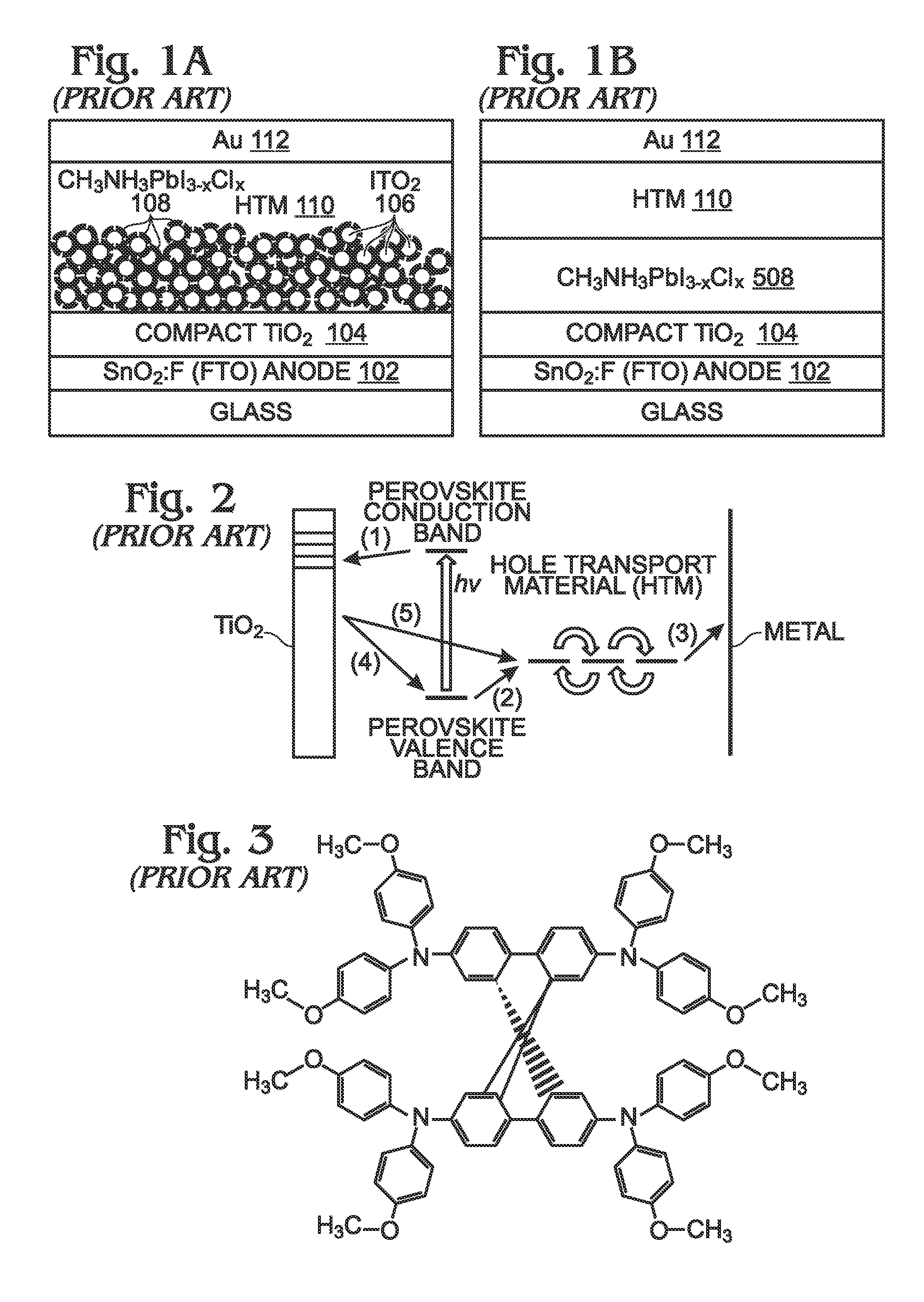
BACKGROUND OF THE INVENTION[0001]1. Field of the Invention[0002]This invention generally relates to solar cells and, more particularly, to a planar structure solar cell, using an inorganic hole-transport material.[0003]2. Description of the Related Art[0004]As evolved from dye-sensitized solar cells (DSSCs), perovskite-sensitized solar-cells have recently attracted a great deal attention with a record high efficiency breakthrough (>17%) based upon low cost organometal trihalide perovskite absorbers. It has been suggested that with the optimization of the cell structure, light absorber, and hole conducting material, this technology could advance to an efficiency that surpasses that of copper indium gallium (di)selenide (CIGS) (20%) and approaches crystalline silicon (25%). Conventional perovskite based solar cells use two common types of architecture: flat and mesoscopic. With the flat architecture, one absorber layer is deposited directly on a flat titanium oxide (TiO2) surface f...

Claims


Application Information

Patent Timeline
IPC IPC(8): H01L51/42H01L51/00
CPCH01L51/4213H01L2031/0344H01L51/0021H01L51/0002Y02E10/549H10K85/00H10K30/152H10K30/211H10K30/151H10K2102/102H10K85/50
Inventor KOPOSOV, ALEXEYZHAN, CHANGQINGPAN, WEI
Owner SHARP LAB OF AMERICA
Learn More