Electrode component with pretreated layers

a technology of electrode layer and layer, applied in the direction of resistor details, current responsive resistors, resistor manufacturing, etc., can solve the problems of high production cost, unsatisfactory bonding strength between silver electrode layer and ceramic substrate, and serious environmental pollution, so as to prolong the operation time and improve the ohmic contact resistance. , the effect of reducing heat generation

Active Publication Date: 2016-02-04
THINKING ELECTRONICS INDAL
View PDF6 Cites 9 Cited by
  • Summary
  • Abstract
  • Description
  • Claims
  • Application Information

AI Technical Summary

Benefits of technology

[0024]3. Enhanced ohmic contact resistance between the electrode layers and the ceramic substrate capable of reduc...

Problems solved by technology

However, conventional silk-screen printing process has the following drawbacks and deficiencies.
1. Lots of toxic substances contained in the organic silver paste cause serious environmental pollution.
2. High production cost arises from the use of a great deal of precious silver material.
1. Low bonding strength due to the silver-ceramic incompatibility. The bonding strength is increased mainly through the glassy substance in the organic silver paste diffused to the grain boundaries of ceramic, such that the bonding strength between the silver electrode layer and the ceramic substrate is not satisfactory.
2. High-resistance ohmic contact.
3. Poor corrosion resistance of the silver electrode layer against lead-free solder. As the solid solubility of silver and tin is relatively high, solder can easily etch a silver layer at a high temperature. Nowadays, owing to the concern of environmental protection, products are manufactured using the lead-free soldering technique. To avoid pseudo soldering and melting silver, the 3Ag solder indicative of a Sn—Ag—Cu solder alloy with a higher silver conte...

Method used


Image

  • Electrode component with pretreated layers
  • Electrode component with pretreated layers
  • Electrode component with pretreated layers

Examples


Embodiment Construction

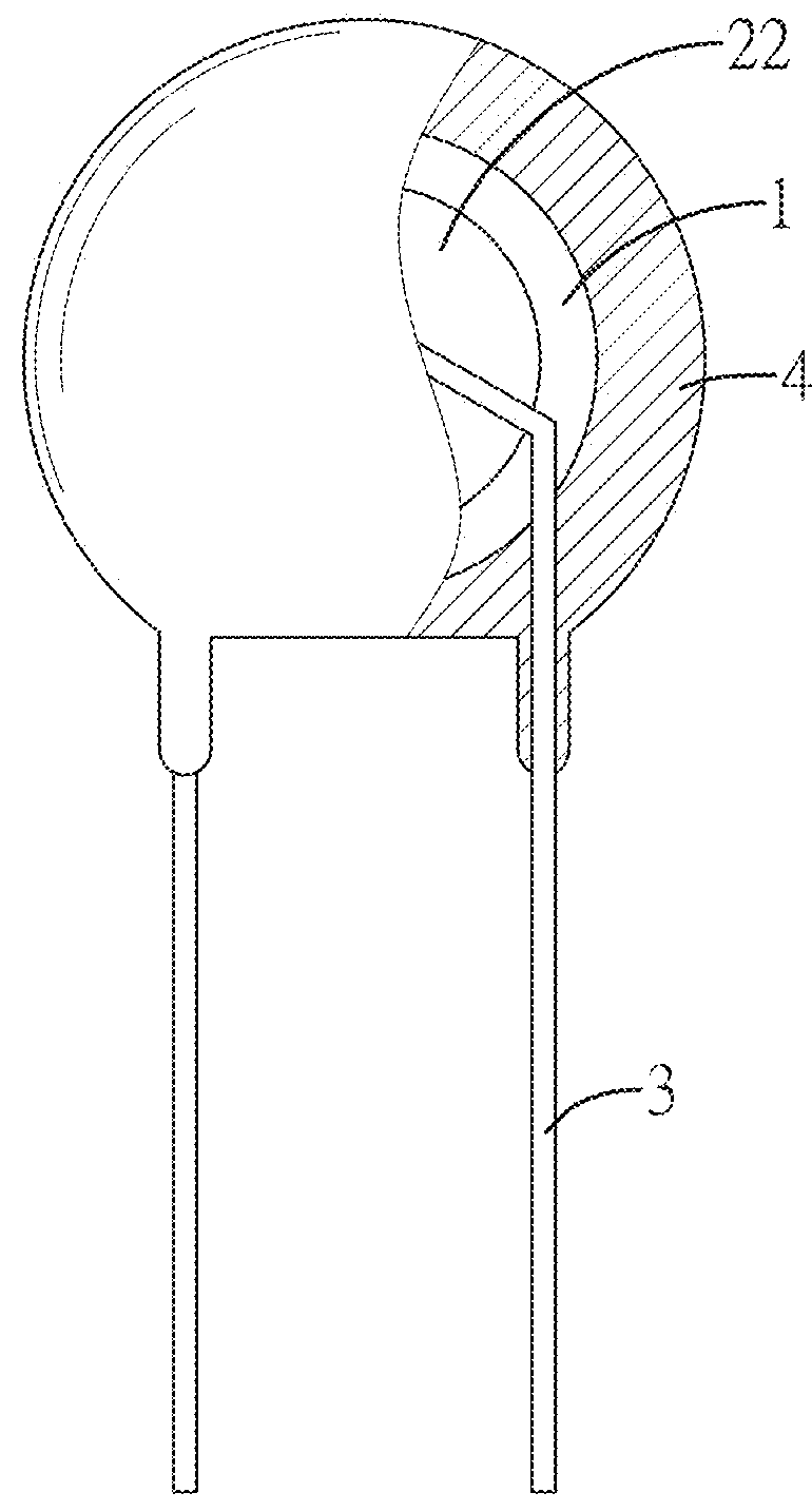
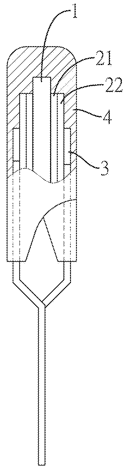
[0034]With reference to FIGS. 1A and 1B, an electrode component with pretreated layers in accordance with the present invention includes a ceramic substrate 1, two pretreated layers 21, two electrode layers 22, two pins 3, and an insulating layer 4.

[0035]The two pretreated layers 21 are respectively formed on two opposite surfaces of the ceramic substrate 1. The two electrode layers 22 are respectively formed on the two pretreated layers 21. The two pins 3 are respectively connected to the two electrode layers 22. The insulating layer 4 encloses the ceramic substrate 1, the pretreated layers 21, the electrode layers 22 and a portion of each pin 3.

[0036]With reference to FIG. 2, a method for fabricating an electrode component is shown. Given the electrode component as a varistor, the method includes processes of spray granulation, dry press forming and ceramic sintering, which are known as conventional techniques and are not repeated here. After the ceramic substrate 1 is made, a pre...


PUM


Abstract

An electrode component with pretreated layers includes a ceramic substrate, two pretreated layers formed on two opposite surfaces of the ceramic substrate, two electrode layers respectively formed on the two pretreated layers, two pins respectively connected to the electrode layers, and an insulating layer enclosing the ceramic substrate, the pretreated layers, the electrode layers, and portions of the two pins. The pretreated layer formed between the ceramic substrate and the electrode layer replaces the fabrication means for conventional silver electrode layer to provide good binding strength between the ceramic substrate and the electrode layer. Besides same electrical characteristics for original products, the electrode component can get rid of the use of precious silver in screen printed silver electrode and avoid pollution caused by evaporation and thermal dissolution of organic solvent while lowering the ohmic contact resistance between the electrode layer and the ceramic substrate.

Description

BACKGROUND OF THE INVENTION[0001]1. Field of the Invention[0002]The present invention relates to an electrode component, and more particularly, to an electrode component with pretreated layers.[0003]2. Description of the Related Art[0004]A varistor is an electronic component mainly formed by zinc oxide powder and mixed with bismuth oxide, antimony oxide, manganese oxide and the like diffused to grain boundaries of zinc oxide. After the mixture is molded by a dry press process, organic binder is removed from the mixture and a ceramic resistor with nonlinear characteristics is generated from the molded mixture using a high-temperature sintering process.[0005]The conductive electrode layer of a conventional varistor is usually formed by the silk-screen printing technique. During fabrication of the electrode layer, a ceramic chip with organic silver paste having a weight percent range of silver 60˜80% attached thereto is processed using a sintering process in a temperature range of 600˜...

Claims


Application Information

Patent Timeline
IPC IPC(8): H01C1/14H01C7/10H01C17/00
CPCH01C1/14H01C17/00H01C7/10H01C1/142H01C1/144H01C7/102H01C17/281H01C17/285H01C17/288
Inventor XU, XUNHUANG, JEN-HENGJIA, ZHIWEI
Owner THINKING ELECTRONICS INDAL
Why Eureka
Try Eureka