Conductive film substrate, transparent conductive film, and method for producing transparent conductive film
- Summary
- Abstract
- Description
- Claims
- Application Information
AI Technical Summary
Benefits of technology
Problems solved by technology
Method used
Image

Examples
first embodiment
Subtractive Method
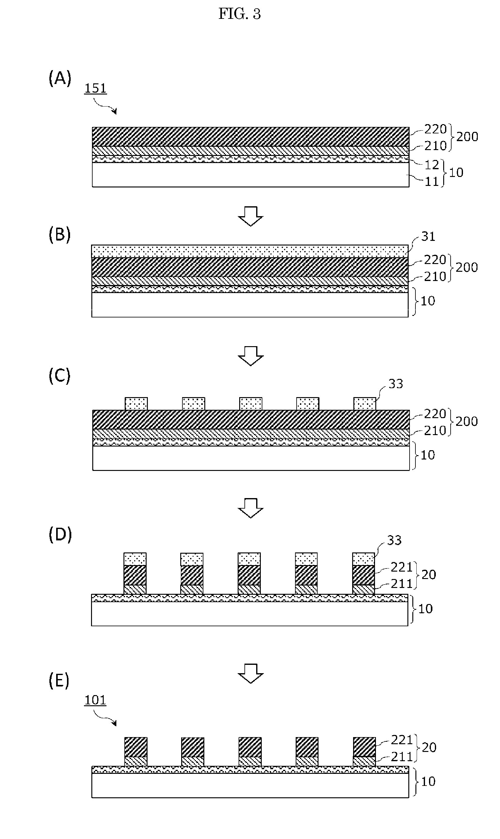
[0039]FIG. 3 is a conceptual view schematically showing one example of a process for producing a transparent conductive film 101. In the aspect shown in FIG. 3, first, a metal layer 200 is formed on a transparent film substrate 10 to give a conductive film substrate 151 (FIG. 3(A)). Thereafter, on the metal layer 200, a resist layer 31 is formed (FIG. 3(B)), and a resist pattern 33 is formed (FIG. 3(C)). Thereafter, a resist pattern-non-formed section of the metal layer 200 is removed by wet etching to form a thin metal wire 20 (FIG. 3(D)). Finally, the resist pattern is removed to give the transparent conductive film 101 (FIG. 3(E)). The series of steps are substantially identical to the steps of a subtractive method in a technique for producing a printed wiring board.
[0040]
[0041]The conductive film substrate 151 includes the metal layer 200 on the transparent film substrate 10.
[0042](Transparent Film Substrate)
[0043]As the transparent film substrate 10, one that ...
second embodiment
Semi-Additive Method
[0083]FIG. 4 is a schematic conceptual view showing another example of a process for producing a transparent conductive film 102. In this embodiment, first, a first metal layer 210 is formed on a transparent film substrate 10 as shown in FIG. 4(A). Thereafter, on the first metal layer 210, a resist layer 35 is formed (FIG. 4(B)), and a resist pattern 37 is formed (FIG. 4(C)). Thereafter, a second metal layer 222 is formed on a resist pattern-non-formed section (FIG. 4(D)), and the resist pattern is removed to give a conductive film substrate 152 with the second metal layer 222 patterned into a thin wire (FIG. 4(E)). Finally, the exposed section of the first metal layer 210 is patterned similarly to the second metal layer 222 by etching to give the transparent conductive film 102 including on a first metal layer 212 thin metal wire 20 having the second metal layer 222 as shown in FIG. 4(F). The series of steps are substantially identical to the steps of a semi-add...
third embodiment
Subtractive Method
[0099]FIG. 5 is a conceptual view schematically showing a process for producing a transparent conductive film 106 including an underlying metal layer 230. In the aspect shown in FIG. 5, first, an underlying metal layer 230 and a metal layer 200 are formed on a transparent film substrate 10 to give a conductive film substrate 156 (FIG. 5(A)). Thereafter, on the metal layer 200, a resist layer 31 is formed (FIG. 5(B)), and a resist pattern 33 is formed (FIG. 5(C)). Thereafter, the metal layer 200 and resist pattern-non-formed section of the underlying metal layer 230 are removed by wet etching to form a thin metal wire 26 (FIG. 5(D)). Finally, the resist pattern is removed to give the transparent conductive film 106 (FIG. 5(E)).
[0100]In the aspect shown in FIG. 5, a transparent conductive film is formed in a process similar to that in the aspect shown in FIG. 3 (subtractive method). In this embodiment, the method for forming the first metal layer and the second metal...
PUM
| Property | Measurement | Unit |
|---|---|---|
| Length | aaaaa | aaaaa |
| Percent by mass | aaaaa | aaaaa |
| Thickness | aaaaa | aaaaa |
Abstract
Description
Claims
Application Information
 - R&D
- Intellectual Property
- Life Sciences
- Materials
- Tech Scout
- Unparalleled Data Quality
- Higher Quality Content
- 60% Fewer Hallucinations
Browse by: Latest US Patents, China's latest patents, Technical Efficacy Thesaurus, Application Domain, Technology Topic, Popular Technical Reports.
© 2025 PatSnap. All rights reserved.Legal|Privacy policy|Modern Slavery Act Transparency Statement|Sitemap|About US| Contact US: help@patsnap.com