
Metal film forming method and conductive ink used in said method

a technology of conductive ink and metal film, which is applied in the direction of resistive material coating, cable/conductor manufacturing, inks, etc., can solve the problems of difficult to completely fill the via hole with a conductive paste, difficulty in forming a viscous paste, and bubbles, etc., to achieve high conduction reliability and simple and easy formation

Inactive Publication Date: 2016-02-25
JSR CORPORATIOON
View PDF2 Cites 17 Cited by
  • Summary
  • Abstract
  • Description
  • Claims
  • Application Information

AI Technical Summary

Benefits of technology

The present invention provides a simple method to easily form a metal film on a surface of a perforated substrate that is adjacent to the hole in the substrate. The invention also provides a conductive ink that can be used in the metal film forming method. The metal film forming method and the conductive ink allow for the high reliability of connecting multiple electrodes together.

Problems solved by technology

However, it is difficult for a viscous paste to completely fill a bottomed blind via having a small diameter without leaving any spaces inside.
Consequently, bubbles may be trapped at times. Thus, the reliable filling of via holes with a conductive paste is difficult, and the air trapped in the via holes problematically causes connection failure.
Further, conductive pastes have low conductivity compared to metallic copper and are difficult to achieve a sufficient electrical connection when applied into small-diameter blind vias.
Because of these facts, the use of conductive pastes is not necessarily an effective approach to reducing the size and increasing the wiring density of printed wiring boards.
However, this method has serious problems in productivity because of the need of complicated treatments such as adding a catalyst to the inner surface in the via holes in order to facilitate the formation of plating layers, and also because of the low rate of the precipitation of the plating films.
In the case of electroplating, great difficulties are encountered in depositing platings only onto the blocked ends of blind vias.
The implementation of such an electroplating treatment with respect to the blocked ends of blind vias while electrically isolating the other portions entails very complicated additional steps (see, for example, Patent Literature 3).
However, the sputtering method has problems in that the treatment entails high vacuum and involves expensive apparatuses.

Method used


Image

  • Metal film forming method and conductive ink used in said method
  • Metal film forming method and conductive ink used in said method
  • Metal film forming method and conductive ink used in said method

Examples


examples

[0142]Embodiments of the present invention will be described in further detail based on Examples hereinbelow without limiting the scope of the invention to such Examples. In the following Examples, “part(s)” indicates “part(s) by mass” unless otherwise mentioned.

Preparation of Conductive Inks

example a1

[0143]At room temperature, 20 parts of copper formate tetrahydrate and 80 parts of 2-ethylhexylamine were mixed with each other with a wave rotor at 50 rpm to give a copper ink having a viscosity of 0.1 Pa·s. The viscosity of the copper ink was measured with an E-type viscometer (RE-80 / 85L manufactured by TOKI SANGYO CO., LTD.) at a temperature of 20° C. and a shear rate of 10 sec−1.

examples a2

to A7

[0144]Copper inks were prepared in the same manner as in Example A1, except that the metal salt and the reducing agent used in Example A1 were changed as described in Table 1, and also that a solvent was used in some of these Examples. The unit for the values describing the amounts of the metal salts, the reducing agents and the solvents in Table 1 is “parts”. The viscosities of the copper inks obtained are shown in Table 1.

TABLE 1Ex. A1Ex. A2Ex. A3Ex. A4Ex. A5Ex. A6Ex. A7MetalCopper formate tetrahydrate201015saltsAnhydrous copper formate1515Copper hydroxide10Copper acetate10Reducing2-Ethylhexylamine80agents2-Ethylhexylpropylamine50353-Ethoxypropylamine7590802-Ethoxyethylamine25Aminoacetaldehyde diethylacetal85Formic acid1510SolventsDiethylene glycol dimethyl ether35Hexyl methyl ether25Viscosity (Pa · s)0.10.0150.010.020.0150.050.02

Manufacturing and Evaluation of Printed Wiring Boards


PUM

PropertyMeasurementUnit
viscosityaaaaaaaaaa
diameteraaaaaaaaaa
temperatureaaaaaaaaaa

Abstract

An object of the invention is to provide a simple method capable of easily forming a metal film on a surface of a perforated substrate that is adjacent to the hole in the substrate. The metal film forming method includes a step of heating a perforated substrate having a hole while a surface of the substrate adjacent to the hole is in contact with a conductive ink containing a metal salt and a reducing agent.

Description

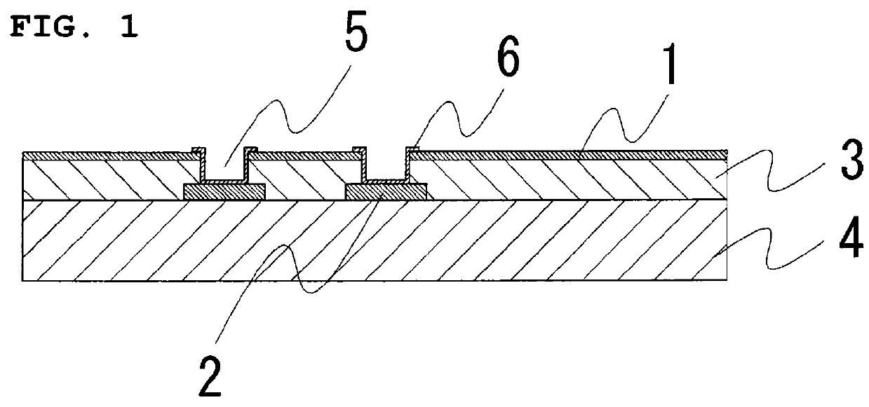
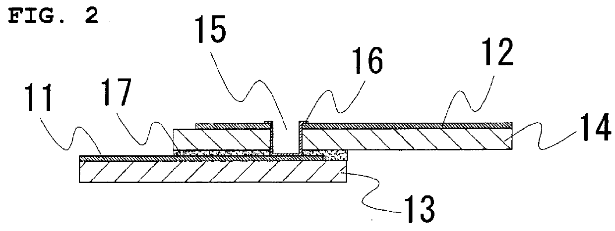
BACKGROUND OF THE INVENTION[0001]1. Field of the Invention[0002]The present invention relates to a method for forming a metal film on a surface of a perforated substrate that is adjacent to the hole in the substrate, to a conductive ink used in the method, and to a multilayer wiring board, a semiconductor substrate and a capacitor cell.[0003]2. Description of the Related Art[0004]In printed wiring boards used in devices such as electronic devices, wiring layers are conductively connected together via metal films formed on the inner surface in bottomed via holes that have an opening on one side and a blocked end on the other side (hereinafter, such via holes will be also written as the “blind vias”). Such metal films are formed by, for example, plating the perforated substrates or filling the via holes with a conductive paste.[0005]For example, a conductive paste is applied into the blind vias with use of a squeegee (see, for example, Patent Literatures 1 and 2). The boards obtained ...

Claims


Application Information

Patent Timeline
Patent Type & Authority Applications(United States)
IPC IPC(8): H05K3/00C08K3/22C08K5/07C08K5/098C08K5/17C09D11/52H01B13/00H01L21/288H01L21/768H01L23/48H01L23/532H05K1/02H05K1/09H10B12/00
CPCH05K3/0091C08K2003/2248H01L23/481H01L21/76898H01L27/1085H01L27/10805H01L23/53228H01L21/288H05K1/097H05K1/0298C09D11/52C08K5/098C08K3/22C08K5/07C08K5/17H05K2201/09509H01B13/0026H05K3/105H05K3/4076H05K2201/0195H05K2201/09545H01L23/49883H01L21/4846H01L28/60H01L2924/0002H01L21/76877C09D11/037C09D11/38H10B12/03H01L2924/00
Inventor SHIMODA, SUGIROUOOKITA, KENZOUARITOME, ISAOWATANABE, KAZUTOTANAKA, KENROU
Owner JSR CORPORATIOON
Learn More