Method for manufacturing crystalline silicon-based solar cell and method for manufacturing crystalline silicon-based solar cell module
- Summary
- Abstract
- Description
- Claims
- Application Information
AI Technical Summary
Benefits of technology
Problems solved by technology
Method used
Image
Examples
first embodiment
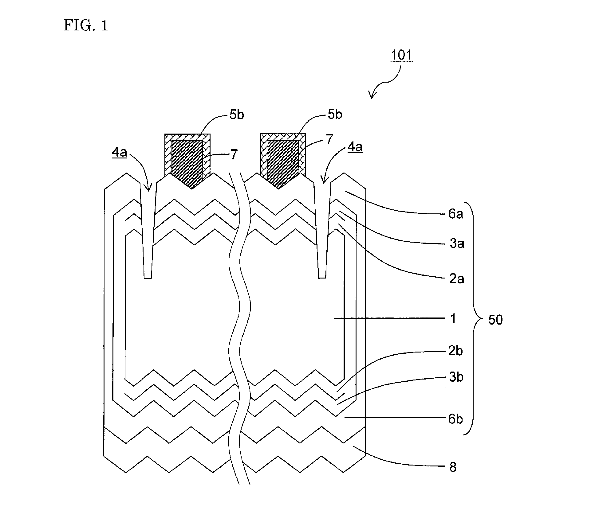
[0057]FIG. 1 is a schematic sectional view showing an example of a heterojunction solar cell according to the first embodiment, in which a protecting layer is provided on a collecting electrode. The heterojunction solar cell 101 of FIG. 1 includes a collecting electrode 7 on a light-receiving side transparent electrode layer 6a of a photoelectric conversion section 50, and the collecting electrode 7 is covered by the protecting layer 5b. An insulation-processed region 4a is formed on the photoelectric conversion section 50.
[0058]<Configuration of Photoelectric Conversion Section]
[0059]On one surface (light-receiving surface or first principal surface) of a crystalline silicon substrate 1 of a first conductivity-type, the heterojunction solar cell 101 has a silicon-based thin-film of an opposite conductivity-type 3a, which has a conductivity type different from that of the crystalline silicon substrate of the first conductivity-type, and a light-receiving side transparent electrode l...
second embodiment
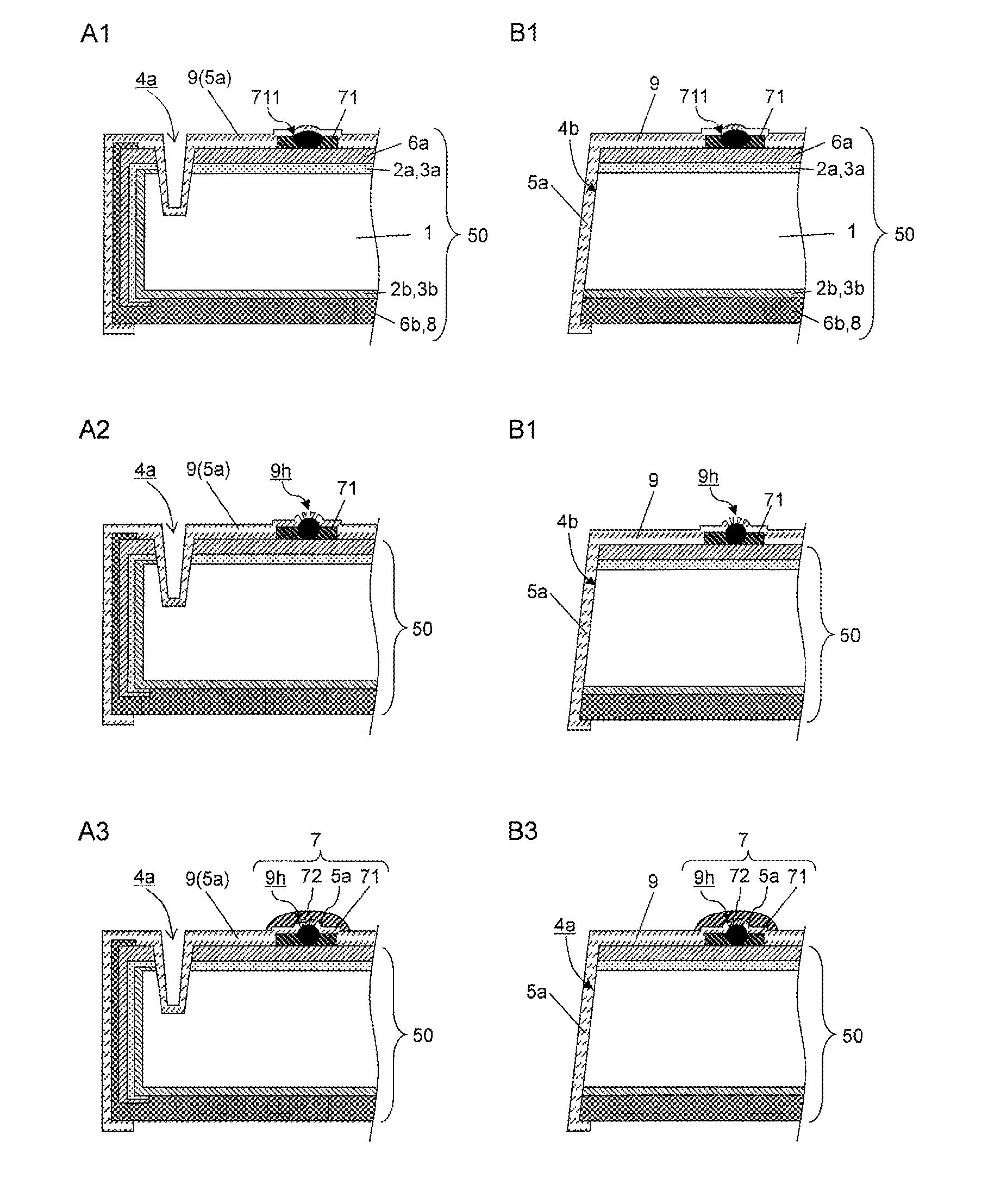
[0144]In the second embodiment of the manufacturing method of the present invention, an insulating material layer is formed on an insulation-processed region as a protecting layer for preventing diffusion of a metal in a collecting electrode. FIG. 9 is a schematic sectional view showing one example of a heterojunction solar cell of the second embodiment, which includes an insulating protecting layer 5a on an insulation-processed region 4a. A heterojunction solar cell 102 shown in FIG. 9 includes a collecting electrode 7 on a light-receiving side transparent electrode layer 6a of a photoelectric conversion section 50. The groove-shaped insulation-processed region 4a is formed on the photoelectric conversion section 50, and the insulating protecting layer 5a is formed on a surface of the insulation-processed region 4a.
[0145]In the second embodiment, the photoelectric conversion section 50, the collecting electrode 7 and the insulation-processed region 4a can be formed in the same man...
PUM
 Abstract
Description
Claims
Application Information


