Oxide semiconductor layer and production method therefor, oxide semiconductor precursor, oxide semiconductor layer, semiconductor element, and electronic device

a production method and semiconductor technology, applied in the direction of non-metal conductors, conductors, organic conductors, etc., can solve the problems of low electron mobility, low element reliability, and variable transistor properties, and achieve excellent electrical property and stability, reduce impurities, and reduce cracks. , the effect of high reliability

Active Publication Date: 2016-06-23
JAPAN ADVANCED INST OF SCI & TECH +1
View PDF4 Cites 14 Cited by
  • Summary
  • Abstract
  • Description
  • Claims
  • Application Information

AI Technical Summary

Benefits of technology

[0024]An exemplary method of producing an oxide semiconductor layer according to the present invention can achieve highly reliable reduction of impurities such as carbon impurities remaining in the oxide semiconductor layer thus produced. It is thus possible to obtain a semiconductor element and an electronic device that have less cracks and are excellent in electrical property and stability. Furthermore, the method of producing the oxide semiconductor layer enables a low-energy production process. An exemplary oxide semiconductor precursor according to t

Problems solved by technology

However, when a polycrystalline silicon film is used, electron scatter at the interface between crystal grains and the like limit electron mobility thereby to cause variation in

Method used


Image

  • Oxide semiconductor layer and production method therefor, oxide semiconductor precursor, oxide semiconductor layer, semiconductor element, and electronic device
  • Oxide semiconductor layer and production method therefor, oxide semiconductor precursor, oxide semiconductor layer, semiconductor element, and electronic device
  • Oxide semiconductor layer and production method therefor, oxide semiconductor precursor, oxide semiconductor layer, semiconductor element, and electronic device

Examples


first embodiment

1. Entire Structure of Thin Film Transistor According to the Present Embodiment

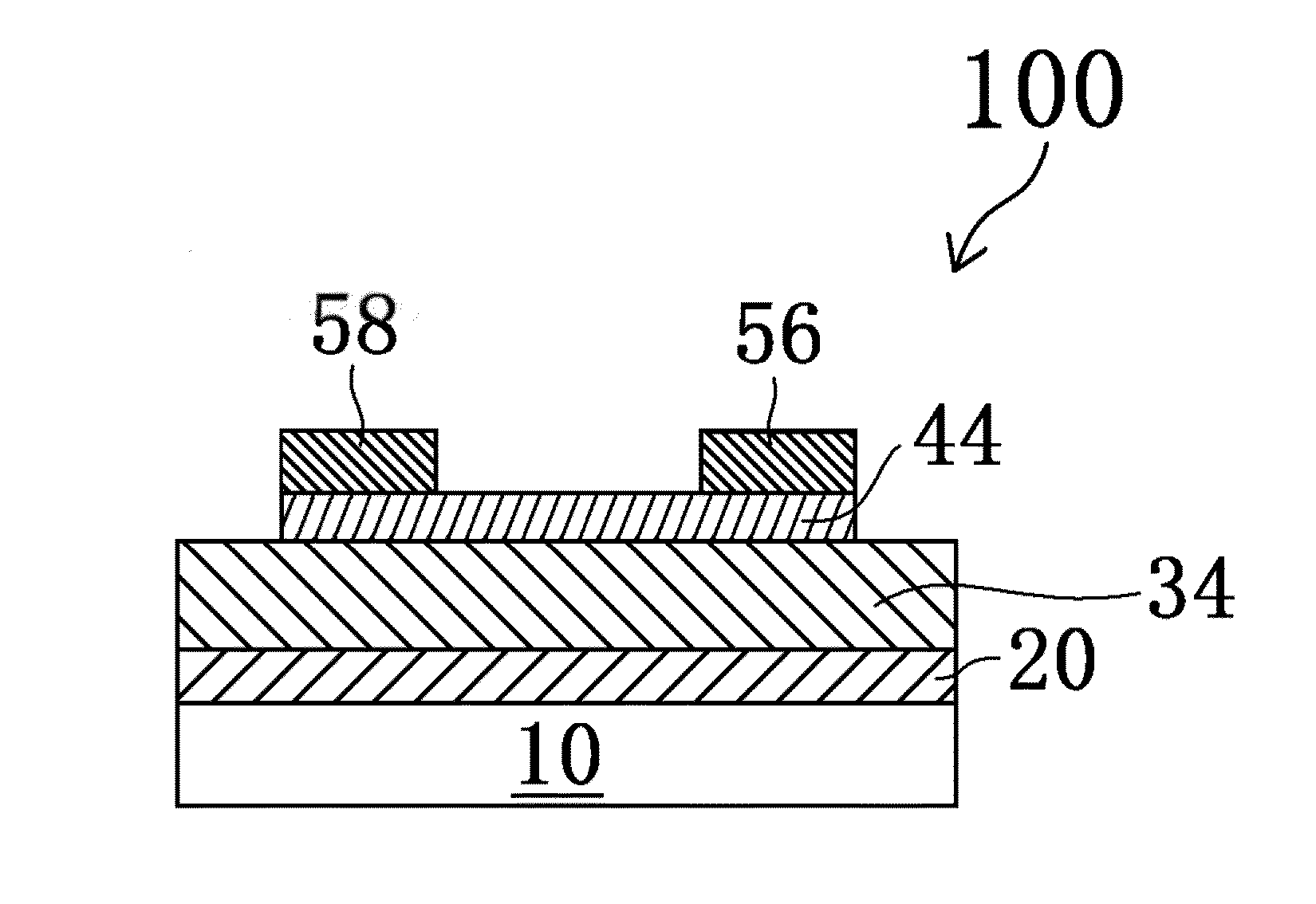
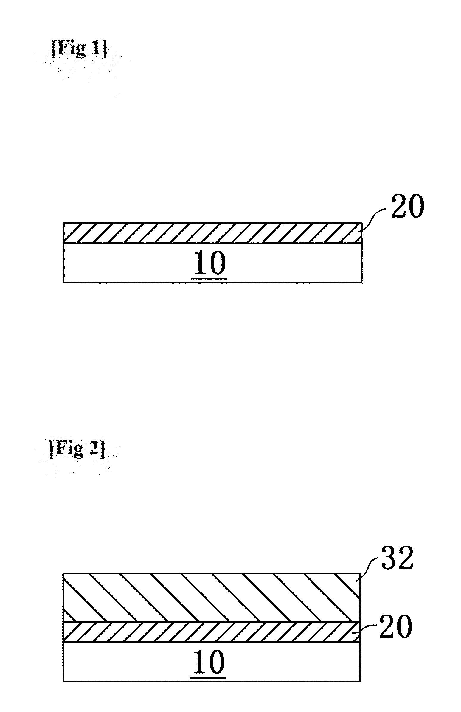
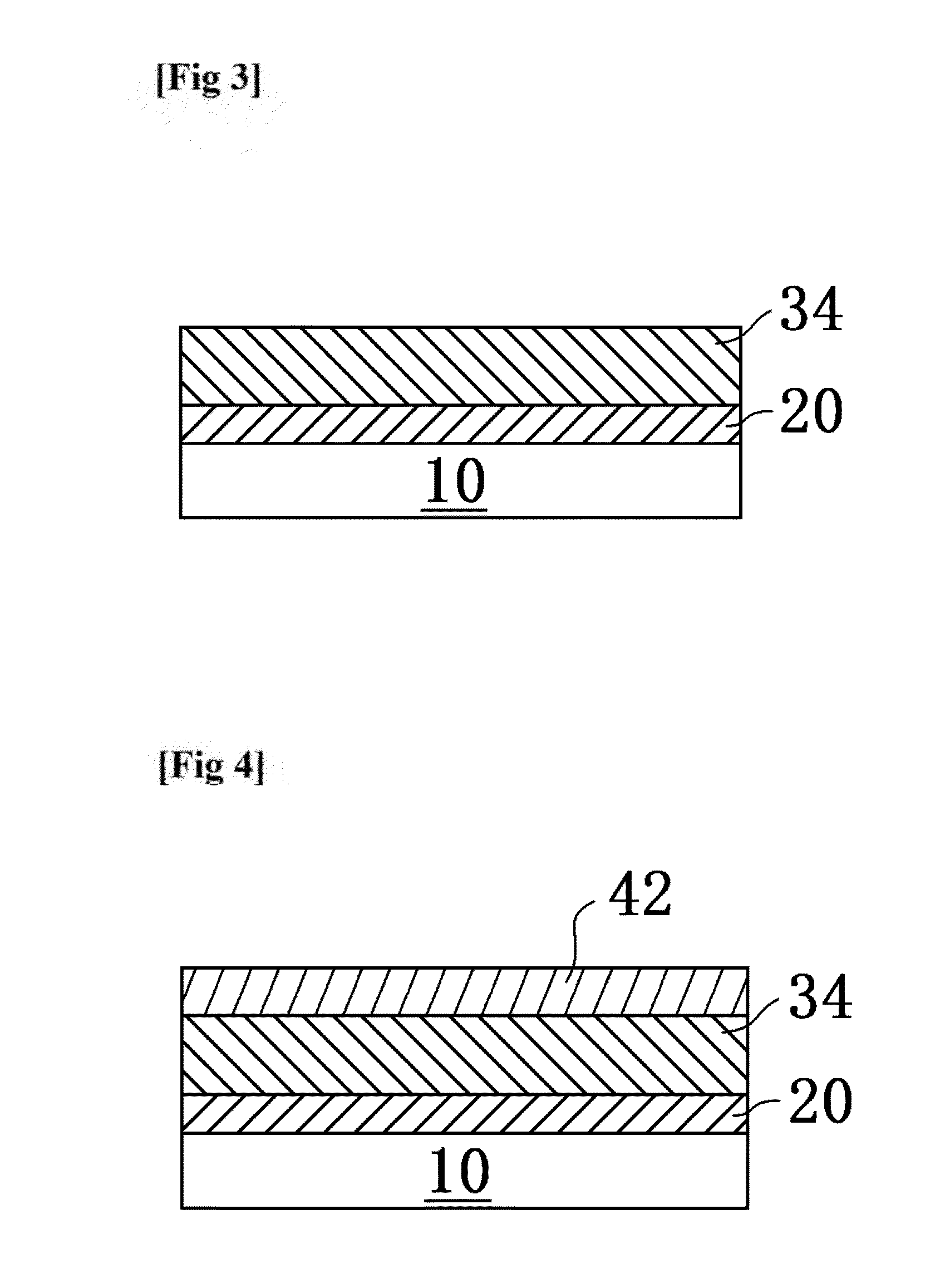
[0060]FIGS. 1 to 8 are schematic sectional views of processes in a method of producing a thin film transistor 100 as an exemplary semiconductor element. FIG. 9 is a schematic sectional view of a process in the method of producing the thin film transistor 100 according to the present embodiment and an entire structure of the thin film transistor. As depicted in FIG. 9, the thin film transistor 100 according to the present embodiment includes a substrate 10, as well as a gate electrode 20, a gate insulator (gate insulating layer) 34, a channel 44, a source electrode 58, and a drain electrode 56, which are stacked on the substrate 10 from the lower side in the mentioned order. A person skilled in the art comprehending the semiconductor element according to the present embodiment can fully comprehend provision or achievement of an electronic device including this semiconductor element (e.g. a mobile terminal,...

modification example of first embodiment

[0119]A thin film transistor according to the present embodiment is similar to the thin film transistor 100 according to the first embodiment in terms of the production steps and the configurations, except that the ultraviolet irradiation step is additionally performed after the step of annealing the channel in the first embodiment (main annealing). Accordingly, the configurations similar to those of the first embodiment will not be described repeatedly.

[0120]In the present embodiment, ultraviolet rays having wavelengths of 185 nm and 254 nm were applied using a known low pressure mercury lamp (manufactured by SAMCO Inc., model: UV-1) after the channel annealing step (main annealing) in the first embodiment. The steps similar to those in the method of producing the thin film transistor 100 according to the first embodiment were performed subsequently. The wavelengths of ultraviolet rays are not particularly limited in the present embodiment. Similar effects can be exerted with ultra...

production example 1

Production of Organozinc Catalyst

[0122]A four-necked flask having a volume of 300 mL and equipped with a stirrer, a nitrogen gas introduction tube, a thermometer, and a reflux condenser was charged with 8.1 g (100 mmol) of zinc oxide, 12.7 g (96 mmol) of glutaric acid, 0.1 g (2 mmol) of acetic acid, and 130 g (150 mL) of toluene. After the atmosphere of the reaction system was replaced with a nitrogen, the temperature of the flask was raised to 55° C. and the materials were stirred at this temperature for four hours so as to cause reaction of the respective materials. The temperature of the flask was then raised to 110° C. and the materials were stirred at this temperature for four hours so as to cause azeotropic dehydration for removal of only water. The flask was then cooled to room temperature so as to obtain a reaction solution including an organozinc catalyst.

[0123]The organozinc catalyst, which was obtained by partially fractionating and filtrating the reaction solution, was s...


PUM


Abstract

The invention provides an oxide semiconductor layer that has less cracks and is excellent in electrical property and stability, as well as a semiconductor element and an electronic device each including the oxide semiconductor layer. The invention provides an exemplary method of producing an oxide semiconductor layer, and the method includes the precursor layer forming step of forming, on or above a substrate, a layered oxide semiconductor precursor including a compound of metal to be oxidized into an oxide semiconductor dispersed in a solution including a binder made of aliphatic polycarbonate, and the annealing step of heating the precursor layer at a first temperature achieving decomposition of 90 wt % or more of the binder, and then annealing the precursor layer at a temperature equal to or higher than a second temperature (denoted by X) that is higher than the first temperature, achieves bonding between the metal and oxygen, and has an exothermic peak value in differential thermal analysis (DTA).

Description

TECHNICAL FIELD[0001]The present invention relates to an oxide semiconductor layer and a production method therefor, an oxide semiconductor precursor, an oxide semiconductor layer, a semiconductor element, and an electronic device.BACKGROUND ART[0002]A thin film transistor (TFT) is a small amplifier tube formed by stacking fine and thin films, and is a three-terminal element including a gate, a source, and a drain.[0003]Conventionally, a polycrystalline silicon film or an amorphous silicon film has typically been adopted as a channel layer of a thin film transistor. However, when a polycrystalline silicon film is used, electron scatter at the interface between crystal grains and the like limit electron mobility thereby to cause variation in transistor property. When an amorphous silicon film is used, electron mobility is very low and an element tends to deteriorate with time thereby to cause lower element reliability. In this regard, an oxide semiconductor has been attracting intere...

Claims


Application Information

Patent Timeline
IPC IPC(8): H01L21/02H01L29/22H01L29/24H01L29/66H01L29/786
CPCH01L21/02614H01L21/02565H01L21/02664H01L29/22H01L29/66969H01L29/7869H01L29/24H01L21/02554C01G15/00H01L21/02628H01L21/02483H01L27/1225
Inventor INOUE, SATOSHISHIMODA, TATSUYAKAWAKITA, TOMOKIFUJIMOTO, NOBUTAKANISHIOKA, KIYOSHI
Owner JAPAN ADVANCED INST OF SCI & TECH
Why Eureka
Try Eureka