Bi-BASED SOLDER ALLOY, METHOD OF BONDING ELECTRONIC COMPONENT USING THE SAME, AND ELECTRONIC COMPONENT-MOUNTED BOARD

a technology of electronic components and alloys, applied in the direction of soldering apparatus, manufacturing tools, printed circuit non-printed electric components association, etc., can solve the problems of pb leakage from products, infiltration into soil, adverse effects, etc., to improve mechanical strength and machinability, improve the wettability of solder, and high joint reliability

Inactive Publication Date: 2016-08-11
SUMITOMO METAL MINING CO LTD
View PDF0 Cites 3 Cited by
  • Summary
  • Abstract
  • Description
  • Claims
  • Application Information

AI Technical Summary

Benefits of technology

[0036]The Bi-based solder alloy of the present invention is substantially free of Pb and has a solidus temperature of 265° C. or more and a liquidus temperature of 390° C. or less. Fine particles including a Ag—Al intermetallic compound are dispersed in the solder alloy. Thus, there can be provided a Bi-based solder alloy that prevents an electronic component from being degraded or damaged by heat during bonding or prevents a remelting problem from being caused by heat during reflow and that has high joint reliability. This Bi-based solder alloy can be suitably used for die bonding, which is a process of making a joint inside an electronic component, or other purposes. Since this Bi-based solder alloy has improved mechanical strength and machinability, it can be formed into a preform wire solder, which then can be wound up. In particular, this Bi-based solder alloy is suitably used as a high-temperature solder alloy preform material for die bonding.
[0037]Further, addition of the above Ag and Al, as well as one or more of P and Ge to this Bi-based solder alloy as added components can improve the wettability of the solder, reduce the occurrence of voids during joining, and prevent a reduction in the strength of joining to a bare Cu frame.
[0038]Further, addition of the above Ag and Al, as well as one or more of Sn and Zn to the Bi-based solder alloy as added components allows the solder alloy to be applied to a Ni-plated lead frame island without reducing the wettability thereof and can prevent a reduction in joint strength after joining an electronic component to the lead frame island.
[0039]Further, by using an electronic component using the Bi-based solder alloy of the present invention or a method for bonding an electronic compound to a board of the present invention, an electronic component-mounted board can be provided that does not cause changes in chip properties or the oxidation of the members and has high mechanical strength.

Problems solved by technology

However, there has been pointed out the risk that after products using a lead (Pb)-containing solder are discarded, Pb could leak from the products, infiltrate into the soil, accumulate in produce and the like, and pose health hazards to humans.
Consequently, adverse effects may occur, including changes in chip properties and the promotion of oxidation of the members.
However, Au—Sn solders are expensive and are not practical in terms of cost.
However, this type of solder has a solidus temperature of less than 265° C. and therefore may cause a problem associated with remelting during mounting.
This solder also has brittle mechanical properties specific to Bi solders.
Accordingly, direct use of this solder has adverse effects on joint reliability, machinability, and the possibility of continuous supply by a device.
Further, this solder has a high liquidus temperature of 400 to 700° C. and therefore may have adverse effects, such as changes in chip properties and the promotion of oxidation of the members.
On the other hand, conventional Bi—Ag solders are supplied only in past form due to the brittle mechanical properties thereof and are insufficient to serve as alternative preform solders in many respects.
However, Ni-plating a lead frame island to be coated with a solder alloy causes problems, including a reduction in the wettability of the solder and a reduction in joint strength resulting from an insufficient joint.
Since the lead frame island has an oxide film thereon, the solder is more likely to wet and spread poorly.
Accordingly, such a solder alloy tends to wet and spread poorly compared to when Ag plating is performed.
That is, a bare Cu frame has a problem that the oxidation of the surface readily proceeds and the solder is more likely to wet and spread poorly thereover due to the influence of the surface roughness.

Method used


Image

  • Bi-BASED SOLDER ALLOY, METHOD OF BONDING ELECTRONIC COMPONENT USING THE SAME, AND ELECTRONIC COMPONENT-MOUNTED BOARD
  • Bi-BASED SOLDER ALLOY, METHOD OF BONDING ELECTRONIC COMPONENT USING THE SAME, AND ELECTRONIC COMPONENT-MOUNTED BOARD
  • Bi-BASED SOLDER ALLOY, METHOD OF BONDING ELECTRONIC COMPONENT USING THE SAME, AND ELECTRONIC COMPONENT-MOUNTED BOARD

Examples


examples

[0110]The present invention will be described in more detail using Examples. However, the present invention is not limited to the Examples. The following measurement and evaluation methods were used in the Examples.

(1) Solidus Temperature and Liquidus Temperature

[0111]The solidus temperature and liquidus temperature were measured using a differential scanning calorimeter (DSC).

(2) Tensile Strength and Elongation

[0112]First, Bi alloys having component compositions shown in Table 1 were melted using a method described below and an atmospheric melting furnace and extruded into 0.75-mm φ preform wire solder samples.

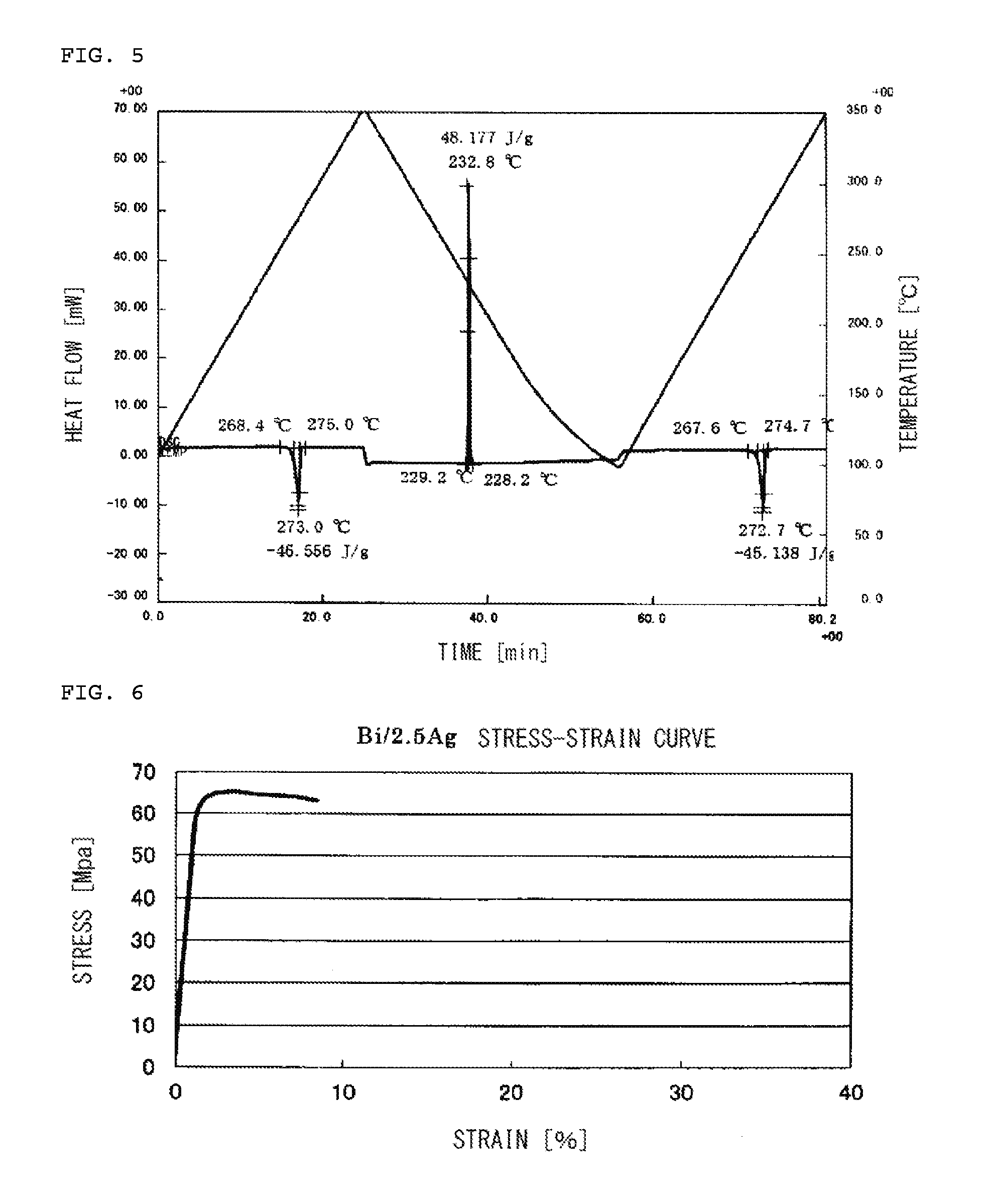
[0113]The obtained 0.75-mm φ wire solders were each cut into a predetermined length and used as a test sample for measuring tensile strength. Each test sample was set in a tensile tester (device name: Tensilon universal tester), and the tensile strength and elongation thereof were measured automatically.

(3) Observation and Particle Diameter of Ag—Al Intermetallic Compound

[011...

examples 1 to 11

[0121](1) Production of Solder Alloys (Preform Solders) for Ag-plated electronic components

[0122]First, Bi, Ag, Al, Te, Cu, and Ni (the purity of each element: 99.99 weight % or more) in the form of 3-mm φ or less shots were provided as raw materials. If any raw material was a large flake or bulk, the size thereof was reduced to 3 mm or less by cutting, crushing, or other means so that, in the melted alloy, the composition did not vary among sampling areas but rather was uniform. Then, a predetermined amount of these raw materials was charged into a graphite crucible for a high-frequency melting furnace.

[0123]Then, the crucible containing the raw materials was put into the high-frequency melting furnace, and nitrogen was passed through the melting furnace at a flow rate of 0.7 L / min or more per kg of the raw materials to suppress oxidation. In this state, the inside of the melting furnace was heated to 500° C. at a temperature rise speed of 5° C. / sec so as to heat and melt the raw m...

examples 12 to 24

(1) Production of Solder Alloys (Preform Solders) for Bare Cu Electronic Components

[0139]Preform wire solders were produced as in the Examples 1 to 11 except that Bi, Ag, Al, P, Ge, and Cu (the purity of each element: 99.99 weight % or more) were used as raw materials. In all these Examples, the solder alloy could be formed into a wire solder, which then could be would up.

(2) Physical Properties and Performance Test

[0140]Using the preform wire solder samples obtained using the above method, the solidus temperature and liquidus temperature were measured. Also, the diameters of particles including a Ag—Al intermetallic compound were observed and measured. Then, each preform solder sample was die-bonded to a Cu lead frame, and the wettability was evaluated. Further, these members were molded using an epoxy resin and then a temperature cycle test and a ref low test were conducted to evaluate the joint reliability. The results are shown in Table 2.


PUM

PropertyMeasurementUnit
melting pointaaaaaaaaaa
diametersaaaaaaaaaa

Abstract

Provided is a Bi-based solder alloy containing a specific amount of Al in Bi—Ag and having particles including a Ag—Al intermetallic compound dispersed therein, a method of bonding a Ag-plated electronic component, a bare Cu frame electronic component, an Ni-plated electronic component, or the like using the same, and an electronic component-mounted board.
A Bi-based solder alloy includes Ag and Al, is substantially free of Pb, and has a Bi content of 80 mass % or more, a solidus of a melting point of 265° C. or more, and a liquidus of 390° C. or less. A content of Ag is 0.6 to 18 mass %, a content of Al is 0.1 to 3 mass %, the content of Al is 1/20 to 1/2 of the content of Ag, and particles including a Ag—Al intermetallic compound are dispersed in the solder alloy.

Description

TECHNICAL FIELD[0001]The present invention relates to a Bi-based solder alloy, a method of bonding an electronic component using the same, and an electronic component-mounted board. More specifically, the present invention relates to a Bi solder alloy that is substantially free of Pb, has a solidus temperature of 265° C. or more and a liquidus temperature of 390° C. or less, and is excellent in machinability, mechanical strength, and joint reliability, a method of bonding a Ag-plated electronic component, a bare Cu frame electronic component, a Ni-plated electronic component, or the like using the same, and an electronic component-mounted board.BACKGROUND ART[0002]Typically, an electronic component, such as a semiconductor device chip, is mounted on a printed board, such as a semiconductor package, by first joining (die-bonding) the electronic component to a lead frame using a solder and then remelting (reflow) the solder.[0003]A Sn / 37mass % Pb eutectic solder (melting point 183° C....

Claims


Application Information

Patent Timeline
Patent Type & Authority Applications(United States)
IPC IPC(8): H05K3/34B23K35/26C22C12/00H05K1/18H05K1/09
CPCB23K35/26H05K3/3457C22C12/00H01L24/29H01L24/32H01L24/48H01L24/73H01L24/83H01L2224/83455H01L2224/83815H01L2924/00014H01L2924/15747H01L2224/29113H01L2224/73265H01L2224/32245H01L2224/48091H01L2224/48247H01L2924/351H01L2924/01322H01L2924/181B23K35/264H05K1/09H05K1/181H05K3/341C22C1/02H01L2224/45099H01L2924/01013H01L2924/01047H01L2924/01032H01L2924/01015H01L2924/0105H01L2924/0103H01L2924/01052H01L2924/01028H01L2924/01029H01L2924/013H01L2924/20107H01L2924/00012H01L2924/00C22C1/03
Inventor NAGATA, HIROAKI
Owner SUMITOMO METAL MINING CO LTD
Why Eureka
Try Eureka